4-layer HDI first-level 3mil bonded PCB
Product Guide | Updated: May 08, 2026 | Reading time: ~7 min
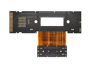
4-Layer HDI First-Level 3mil Bonded Flexible PCB
The 4-layer HDI first-level 3mil bonded PCB from Well Circuits is a high-performance flexible circuit solution engineered for extreme miniaturization and robust connectivity. Featuring High-Density Interconnect (HDI) technology with 3mil laser-drilled microvias, this advanced flexible PCB is designed to accommodate complex component layouts in exceptionally compact spaces. It offers superior signal integrity and reliability, making it an ideal choice for cutting-edge applications where space is at a premium and circuit flexibility is essential. Trust Well Circuits for precision manufacturing adhering to stringent IPC standards.
Key Technical Specifications
| Specification | Detail |
|---|---|
| Layer Count | 4 Layers |
| Board Type | Flexible PCB (FPC) with HDI |
| HDI Structure | 1+2+1 (First-level microvias) |
| Microvia Size | 3mil (0.075mm) Laser-drilled |
| Minimum Line Width/Spacing | 2/2 mil (0.05/0.05 mm) |
| Minimum Mechanical Drill Size | 6mil (0.15mm) |
| Base Material | Polyimide (PI) |
| Copper Thickness | 1/3 oz, 1/2 oz, 1 oz (per IPC-6012 guidelines) |
| Coverlay/Solder Mask | Polyimide Coverlay (Yellow, Black, White), Solder Mask (Green, Black, White) |
| Surface Finish | ENIG (Electroless Nickel Immersion Gold), OSP (Organic Solderability Preservative), Immersion Silver |
| Impedance Control | ±10% (TDR tested) |
| Outline Tolerance | ±0.1mm (Routing), ±0.05mm (Laser Cutting) |
| Maximum Panel Size | 250mm x 500mm (typical, custom sizes available) |
| Quality Standard | IPC Class 2 / IPC Class 3 (specify at order) |
| Testing | 100% Automated Optical Inspection (AOI), 100% Electrical Test (E-Test) |
Target Applications
The compact size, inherent flexibility, and high-density capabilities of our 4-layer HDI first-level 3mil bonded flexible PCBs make them indispensable across a wide array of advanced industries:
- Consumer Electronics: High-end smartphones, wearables (smartwatches, fitness trackers), augmented/virtual reality devices, and compact cameras requiring maximum component density in minimal space.
- Automotive Electronics: Advanced driver-assistance systems (ADAS), infotainment systems, flexible displays, and sensor modules within confined automotive environments, often requiring AEC-Q grade reliability.
- Medical Devices: Implantable electronics, diagnostic tools, portable patient monitoring systems, endoscopy cameras, and hearing aids where miniaturization and biocompatibility are paramount.
- Industrial IoT (IIoT): Miniaturized sensors, smart factory equipment, robotics, and drones that demand robust, high-density flexible interconnections for reliable data acquisition and control.
- Aerospace & Defense: Lightweight avionics, satellite components, and portable communication systems where reliability, space-saving, and resistance to harsh conditions are critical.
- Data Communications: High-speed data links in compact servers, networking equipment, and portable computing solutions, benefiting from superior signal integrity and reduced form factor.
Why Choose Well Circuits?
- Uncompromising Quality Standards: Our ISO 9001:2015 certified facility ensures every flexible PCB is manufactured to the highest quality. We produce boards compliant with IPC-6012 (Qualification and Performance Specification for Flexible Printed Boards) and inspect them according to IPC-A-610 (Acceptability of Electronic Assemblies) Class 2 or Class 3, as specified by your design, ensuring robust performance and longevity.
- Advanced HDI Expertise: Specializing in complex HDI flexible circuits, Well Circuits employs state-of-the-art equipment and deep technical knowledge to produce boards with 3mil laser-drilled microvias and fine line geometries. This enables maximum component density and superior signal integrity, crucial for today’s high-performance applications.
- Rigorous Testing & Inspection: To guarantee functionality and integrity, every 4-layer HDI flexible PCB undergoes 100% Automated Optical Inspection (AOI) and comprehensive Electrical Testing (E-Test) before shipment. This stringent process ensures a defect escape rate below 0.5%, providing you with confidence in every delivery.
- Reliable Lead Times & Dedicated Support: From rapid prototyping to high-volume production, we are committed to delivering your projects on schedule. Standard sample lead times are typically 3-5 working days, with mass production completed within 5-15 working days. Our dedicated technical support team is always available to assist with design and manufacturing queries, adhering to guidelines like IPC-2221 for generic design standards.
Pricing & Lead Time
The cost and lead time for your 4-layer HDI first-level 3mil bonded flexible PCBs are meticulously determined by specific design parameters, chosen material options, order volume, and the required IPC class. While our standard sample lead times are typically 3-5 working days and mass production 5-15 working days, we encourage you to submit your Gerber files and detailed specifications for a precise and competitive quotation tailored to your project’s unique requirements. Our team is ready to provide a transparent and efficient quote to help bring your innovative designs to life.
Need a Quote?
Fill in your requirements and get a detailed quotation within 24 hours.
Request a QuoteNo account required • Free consultation
Request a Quote
Fill in your requirements and we'll get back to you within 24 hours.