PCB Capability
WellCircuits has established in-depth cooperation with well-known domestic and foreign enterprises in the communication industry for a long time and provides high-quality, stable and reliable communication PCB products.
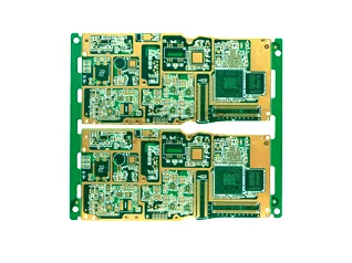
The application fields of communication PCBs mainly cover four aspects: wireless networks (communication base stations), transmission networks, data communications, and fixed broadband networks, which meet the requirements of information transmission and communication. Communication PCBs pursue characteristics such as high speed and high frequency, and they have the features of high-speed signal transmission and strong anti-interference ability to ensure the stability and reliability of communication equipment. Well Circuits engineers have accumulated rich research and development experience in high-speed multi-layer PCB, high-frequency microwave PCB, alumina/aluminum nitride ceramic PCB, optical module, back drilling, backplane, thick copper plate, buried copper block, multifunctional metal substrate, etc., proficient in high-frequency and high-speed material properties, professional research on signal integrity and impedance control. And have the ability to test independently.


-
4-layer high-frequency mixed plating edge coating pcb
评分 0 / 5
Product De…
-
10-layer HDI second order PCB
评分 0 / 5
Product De…
-
28-layer high-speed Panasonic M7 back-drill PCB
评分 0 / 5
Product De…

-
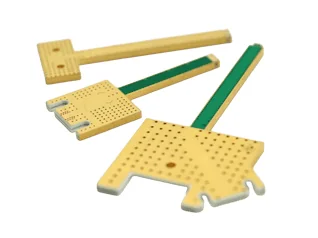
4-layer high-frequency pure pressure
评分 0 / 5
Product De…
