
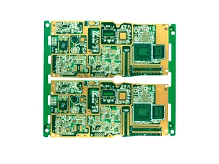
10-layer HDI second order PCB
Product Guide | Updated: May 08, 2026 | Reading time: ~12 min
10-layer HDI second order PCB
The 10-layer HDI second order PCB from Well Circuits represents a pinnacle in flexible printed circuit board (FPC) technology, engineered for the most demanding, space-constrained applications. Manufactured in our ISO 9001-certified facility, this advanced FPC integrates High-Density Interconnect (HDI) techniques with second-order microvias, enabling significantly higher component density and superior electrical performance in a flexible format. Designed for engineers and procurement managers seeking reliable, specification-driven solutions, it is ideal for miniaturized consumer electronics, complex telecommunication modules, and high-reliability automotive systems. All builds adhere strictly to IPC — Institute for Printed Circuits standards, with options for IPC Class 2 or Class 3 at order.
Key Takeaways
- Target applications: smartphones, tablets, automotive electronics, medical devices, IoT hardware, telecommunication infrastructure, industrial control systems
- IPC Class 2 and IPC Class 3 certified builds available — specify at order
- Minimum line width/spacing: 2/2 mil (0.05 mm) on advanced lines for ultra-fine routing
- Every board undergoes AOI (Automated Optical Inspection), electrical testing, and X-ray inspection before shipment
- Standard sample lead time: 3-5 working days; mass production: 5-15 working days
- ISO 9001 quality system — defect escape rate below 0.5%, tracked monthly
Trusted by Engineers Worldwide
| Certification / Standard | Description | Relevance |
|---|---|---|
| ISO 9001:2015 | Quality management system — verified annually by third-party auditor | All production processes, ensuring consistent quality and continuous improvement. |
| IPC-6012 Class 2 / 3 | Performance specification for rigid and flexible printed boards. Class 2 for general electronic products, Class 3 for high-reliability/harsh environment applications. | Defines the performance and reliability criteria for manufactured PCBs, ensuring compliance with industry benchmarks. |
| IPC-A-610 Class 2 / 3 | Acceptability of Electronic Assemblies. Class 2 for general, Class 3 for high-reliability. | Specifies criteria for the visual quality and workmanship of PCB assemblies, providing a benchmark for inspection. |
| IPC-2221 / IPC-2223 | Generic Standard on Printed Board Design / Sectional Design Standard for Flexible Printed Boards. | Provides guidelines for the design of PCBs, ensuring manufacturability, performance, and reliability from the initial design phase. |
| AEC-Q100 / AEC-Q200 | Automotive Electronics Council standards for stress testing of integrated circuits and passive components. | Ensures components and PCBs meet the stringent reliability requirements for automotive environments. |
Key Specifications: 10-Layer HDI Second Order FLEX PCB
Our 10-layer HDI second order flexible PCBs are engineered to meet precise design requirements for complex, high-performance applications. Below are the typical specifications; custom options are available upon request.
| Specification | Detail | Notes |
|---|---|---|
| Layer Count | 10 Layers | Optimal for complex routing and signal integrity. |
| PCB Type | Flexible Printed Circuit Board (FPC) with HDI (2nd Order) | Utilizes stacked microvias for maximum routing density. |
| HDI Structure | 2+N+2 (Second Order) | Two layers of microvias on each side of the core, enabling advanced routing and miniaturization. |
| Base Material | Polyimide (PI) Film | Excellent flexibility, thermal stability, and electrical properties. |
| Copper Weight (Internal) | 0.5 oz (18 µm), 1 oz (35 µm) | Standard options; heavier copper available for power applications. |
| Copper Weight (External) | 0.5 oz (18 µm), 1 oz (35 µm) | Ensures robust connections and current carrying capacity. |
| Minimum Line Width/Spacing | 2 mil / 2 mil (0.05 mm / 0.05 mm) | Achieves ultra-fine pitch component placement and high routing density. |
| Minimum Laser Drill Hole Size | 4 mil (0.1 mm) | For microvias, critical for HDI designs. |
| Minimum Mechanical Drill Hole Size | 6 mil (0.15 mm) | For through-holes and larger vias. |
| Minimum Annular Ring | 3 mil (0.075 mm) | Ensures reliable connection between via and pad. |
| Surface Finish Options | ENIG (Electroless Nickel Immersion Gold), ENEPIG, Immersion Gold, Immersion Silver, OSP (Organic Solderability Preservatives) | Various finishes to suit different assembly processes and environmental requirements. |
| Solder Mask/Coverlay | Flexible Photoimageable Solder Mask (FPSM), Polyimide Coverlay | Protects circuitry while maintaining flexibility. |
| Impedance Control | Yes, ±10% Tolerance | Crucial for high-speed signal integrity, verified by TDR. |
| Dielectric Constant (Dk) | Typically 3.3 - 3.5 (for PI) | Ensures consistent signal propagation. |
| Maximum Panel Size | Up to 250 x 500 mm (depending on design complexity) | Accommodates various production volumes and board sizes. |
| Routing / Profile Tolerance | ±0.1 mm (Mechanical), ±0.05 mm (Laser) | High precision for complex board shapes. |
| IPC Standard Compliance | IPC-6012 Class 2 or Class 3 | Ensures adherence to industry-recognized quality and reliability standards. |
Advanced Flexible HDI Technology
The 10-layer HDI second order flexible PCB stands at the forefront of interconnect technology. "Second order" HDI refers to the use of stacked microvias (e.g., via-in-pad-in-pad structures), which allows for even greater routing density and miniaturization compared to single-layer HDI. This capability is essential for compressing complex circuitry into minimal space, a requirement for next-generation portable devices and compact modules. Coupled with the inherent flexibility of polyimide, these PCBs offer unparalleled design freedom, enabling dynamic bending and intricate 3D packaging solutions.
Furthermore, our capabilities extend to Every Layer Interconnect (ELIC) HDI, providing direct electrical connections between any two adjacent layers. This technology further optimizes signal paths, reduces parasitic effects, and enhances overall circuit performance, making our ELIC HDI PCBs ideal for high-frequency and high-speed applications where signal integrity is paramount.
Applications
The versatility and high performance of our 10-layer HDI second order flexible PCBs make them indispensable across a broad spectrum of industries:
- Consumer Electronics: High-end smartphones, tablets, smartwatches, and other wearable devices requiring extreme miniaturization and flexibility.
- Automotive Electronics: Advanced driver-assistance systems (ADAS), infotainment systems, battery management systems (BMS) in EVs, and compact sensor modules where space and reliability are critical.
- Medical Devices: Implantable devices, diagnostic equipment, portable medical monitors, and surgical tools demanding high reliability and compact form factors.
- Telecommunication Infrastructure: 5G modules, high-frequency antenna arrays, and data center equipment requiring superior signal integrity and density.
- IoT Hardware: Compact sensors, smart home devices, and industrial IoT nodes where space is at a premium and environmental resilience is needed.
- Aerospace & Defense: Miniaturized avionics, satellite components, and military communication systems that require robust, high-performance, and lightweight PCBs.
Why Choose WellCircuits for Your Flexible HDI PCBs?
- Unmatched Expertise: With years of experience in advanced PCB manufacturing, our engineering team possesses deep knowledge in HDI and flexible circuit design and production, ensuring optimal solutions for your most complex projects.
- Rigorous Quality Control: Every board undergoes comprehensive testing, including Automated Optical Inspection (AOI), 100% electrical test, and X-ray inspection to guarantee defect-free delivery and adherence to IPC-A-610 acceptability criteria.
- Advanced Manufacturing Capabilities: Our state-of-the-art facility is equipped with precision laser drilling, fine line imaging, and advanced lamination technologies essential for producing 2nd order HDI and ELIC flexible PCBs with exceptional accuracy.
- Commitment to Standards: We operate under an ISO 9001:2015 certified quality management system, and all products are built to IPC-6012 Class 2 or Class 3 standards, ensuring reliability and performance for critical applications.
Pricing & Lead Time
Pricing for our 10-layer HDI second order flexible PCBs is custom-quoted based on the complexity of your design, material selection, and order volume. We offer competitive pricing while maintaining the highest quality standards. Our efficient production processes ensure rapid turnaround times:
- Sample Lead Time: Typically 3-5 working days
- Mass Production Lead Time: Typically 5-15 working days
Contact us today with your design specifications for a detailed and accurate quote.
{"@context":"https://schema.org","@graph":[{"@type":"TechArticle","@id":"https://www.wellcircuits.com/pcb-product/10-layer-hdi-second-order/#techarticle","headline":"10-layer HDI second order PCB","description":"10 layer HDI second order PCB: Comprehensive technical overview covering design considerations, materials selection, and quality standards. Request a quote t...","url":"https://www.wellcircuits.com/pcb-product/10-layer-hdi-second-order/","inLanguage":"en-US","isPartOf":{"@id":"https://www.wellcircuits.com/pcb-product/10-layer-hdi-second-order/#webpage"},"author":{"@type":"Person","@id":"http://www.wellcircuits.com/#/schema/person/1","name":"even","url":"http://www.wellcircuits.com"},"publisher":{"@id":"http://www.wellcircuits.com/#organization"},"datePublished":"2024-12-02T10:18:33+08:00","dateModified":"2026-06-24T12:04:59+08:00","image":{"@id":"https://cdn.wellcircuits.com/wp-content/uploads/2024/12/20240131093750_2.webp"}},{"@type":"QAPage","@id":"https://www.wellcircuits.com/pcb-product/10-layer-hdi-second-order/#qapage","mainEntity":{"@id":"https://www.wellcircuits.com/pcb-product/10-layer-hdi-second-order/#techarticle"}},{"@type":"Organization","@id":"http://www.wellcircuits.com/#organization","name":"WellCircuits","url":"http://www.wellcircuits.com","logo":{"@type":"ImageObject","url":"https://cdn.wellcircuits.com/wp-content/uploads/2025/03/wellcircuits-logo.png"}},{"@type":"Person","@id":"http://www.wellcircuits.com/#/schema/person/1","name":"even","url":"http://www.wellcircuits.com","jobTitle":"PCB Manufacturing Engineer","worksFor":{"@id":"http://www.wellcircuits.com/#organization"}}]}
Need a Quote?
Fill in your requirements and get a detailed quotation within 24 hours.
Request a QuoteNo account required • Free consultation

Request a Quote
Fill in your requirements and we'll get back to you within 24 hours.