Published: February 04, 2026 | Reading time: ~19 min
Most engineers assume that if the schematic is right and the firmware runs, the hard work is done. That’s the comfortable myth. In reality, a lot of boards die quietly because the PCB boards underneath were treated as an afterthought—too thin copper, the wrong Tg, sloppy return paths.
The uncomfortable truth is that the printed circuit board carries far more responsibility than most people give it credit for. It handles current, spreads heat, controls impedance, survives reflow, and gets blamed when something resets at 80°C. I’ve watched teams chase phantom firmware bugs for weeks, only to discover the board itself was the real problem.
This article breaks PCB boards down the way working engineers think about them. What they’re actually made of, why different types exist, how manufacturing and materials change behavior, and where design decisions come back to bite you. From embedded systems to repair, prototyping, legislation, and even recycling, the goal here isn’t theory—it’s helping you make boards that survive real-world use. Insights are drawn from day-to-day industry practice, including observations common among fabricators like WellCircuits, where design assumptions meet manufacturing reality.
1. When a “Simple Board” Isn’t Simple Anymore
The board looked fine on paper. Power LED lit up. The microcontroller was programmed without a fight. Then it went into thermal test and reset itself at around 78–82°C. Not a schematic issue. Not firmware. The problem was the pcb board itself—trace width too skinny, copper weight underestimated, and no real thought given to heat spreading.
I’ve seen this pattern more times than I can count. People treat pcb boards like passive furniture, just something to hold parts together. That’s a mistake. A printed circuit board is an active part of the electrical and thermal system. Ignore that, and the board will remind you—usually late in the schedule.
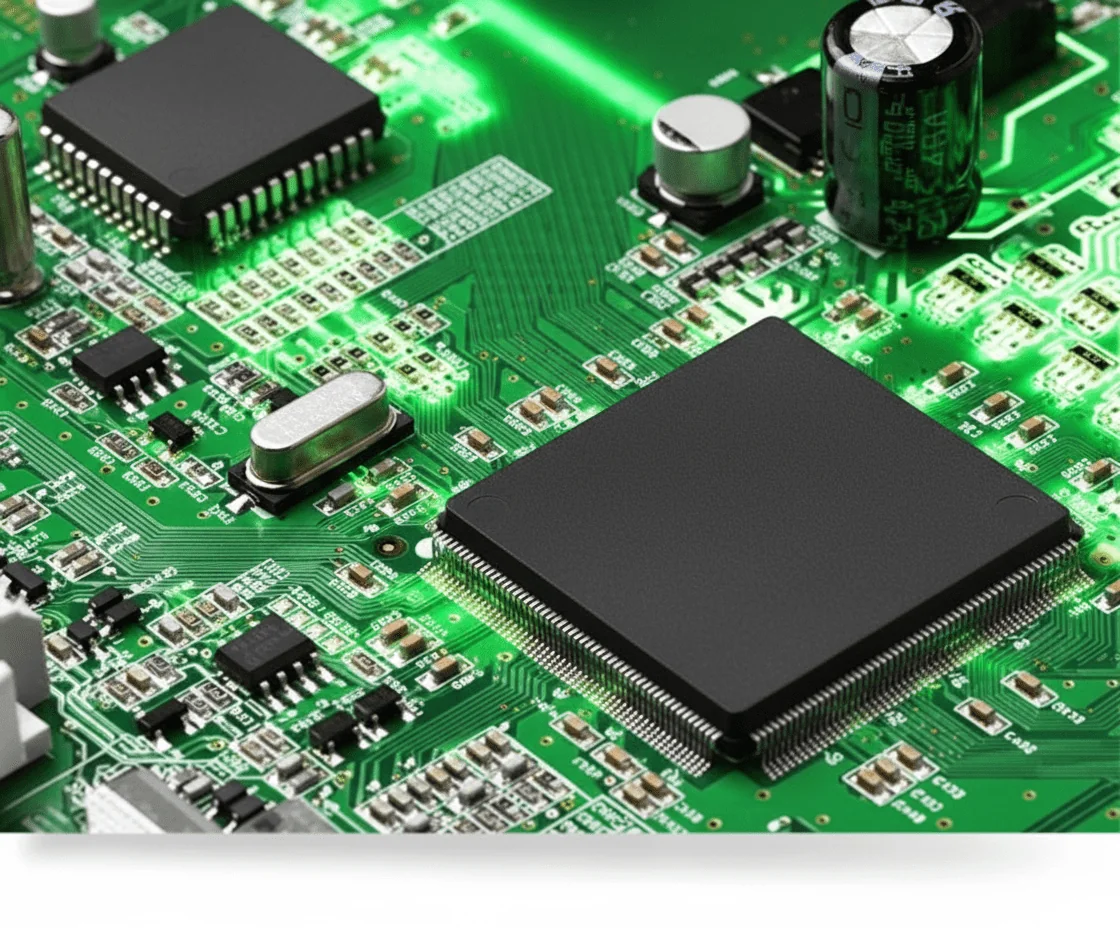
At its core, a PCB is a flat insulating substrate with copper features patterned to route signals, distribute power, and mechanically support components. Fiberglass-reinforced epoxy (FR-4) is still the workhorse material, but “flat board with copper” undersells what’s really going on. That copper controls impedance. The stackup controls EMI. The board thickness and glass weave affect reliability under thermal cycling.
I’m biased toward designs that respect the board early. When engineers do, yield problems tend to stay boring. When they don’t, everyone suddenly becomes very interested in re-spins and expedited pcb boards manufacturing.
2. How PCBs Quietly Carry the Whole System
Here’s a data point that surprises juniors: in a typical embedded product, over 60–70% of field failures trace back to interconnects, not silicon. Solder joints, vias, pads, copper traces. That’s all PCB territory.
A pcb circuit board doesn’t just connect components—it defines how signals behave. High-speed digital lines don’t “flow” so much as they interact with reference planes. Power integrity depends on plane capacitance, not just decoupling caps. Even low-frequency designs suffer if return paths are sloppy.
Signal transmission on a PCB happens through etched copper conductors. Width, spacing, copper thickness, and dielectric constant all matter. Change any of those and rise times, crosstalk, and losses shift. Usually a little. Sometimes, it’s enough to fail EMC testing by a painful margin.
In embedded systems, PCBs also handle mechanical stress. Buttons get pressed. Cables get yanked. Boards flex during assembly. If the layout ignores strain relief or places vias too close to pads, cracks show up after a few hundred thermal cycles.
| PCB Function | What It Actually Controls | What Goes Wrong When Ignored |
|---|---|---|
| Signal routing | Impedance, skew, noise coupling | Intermittent data errors, EMI failures |
| Power distribution | Voltage stability, transient response | Random resets, ADC noise |
| Mechanical support | Component alignment, solder stress | Cracked joints, early-life failures |
3. What Are PCB Boards Really Made Of?
People ask this all the time, usually after a board warps in reflow: what are pcb boards made of, anyway?
Most boards you’ll touch are FR-4—woven fiberglass cloth impregnated with epoxy resin. Copper foil gets laminated to it under heat and pressure. That’s the baseline. From there, things branch out: high-Tg FR-4 for lead-free soldering, polyimide for high-temperature environments, and aluminum-backed boards for LEDs.
- Substrate: FR-4 (Tg 130–180°C typically), polyimide, or metal-core
- Copper: 0.5oz to 2oz common; heavier copper costs more and etches worse
- Surface finish: HASL, ENIG, OSP—each with shelf-life and reliability trade-offs
Forget marketing claims. Material choice is about operating temperature, frequency, and mechanical abuse. If someone pushes Rogers for a 1GHz design, I push back.
4. The Most Common PCB Type Mistake
Here’s the mistake: defaulting to a single-layer board because it’s “cheaper.” It usually isn’t.
Single-sided boards look cost-effective on a quote, but they force ugly routing, jumpers, and long return paths. Assembly labor goes up. EMI risk goes up. Debug time definitely goes up. By the time it ships, the savings are mostly gone.
Types of PCB boards exist for a reason. Single-sided works for very simple power or LED boards. Double-sided handles moderate density well. Multilayer boards—four layers and up—buy you clean power planes and controlled impedance.
Yes, multilayer boards cost more per unit. Roughly 1.6–2.2× going from two to four layers, depending on volume and stackup. But they often save weeks of engineering time. I’ll take that trade in most cases.
5. A Practical Look at Common PCB Board Types
Not all boards earn their complexity. Over-design is just as real as under-design.
Single-sided boards still make sense for low-cost consumer products where currents are modest, and signal integrity isn’t critical. Double-sided boards are the everyday workhorse—appliances, control panels, basic IoT nodes.
Multilayer boards shine when signal speed climbs or when analog and digital have to coexist. Six layers isn’t exotic anymore, but beyond eight layers, costs rise fast, and not every shop can hold tight registration.
Metal-core boards, often aluminum, are popular for LED lighting. They spread heat well, but drilling and isolation routing are slower. Copper-core is better thermally, but heavy, expensive, and usually overkill below roughly 3–4 W/cm².
I’ve seen WellCircuits and similar mid-volume fabricators handle all of these reliably, but capability still varies. Always ask what they actually build every week, not what’s on the website.
6. Dimensions, Thickness, and Why They Matter More Than You Think
Board size isn’t just about fitting the enclosure. Thickness affects impedance, rigidity, and assembly yield.
The “standard” 1.6mm board exists because it balances stiffness and manufacturability. Thinner boards—1.0–1.2mm—flex more and need care around connectors. Thicker boards—2.0mm and up—cost more and can cause soldering issues with fine-pitch parts.
| Thickness Range | Typical Use | Trade-Offs |
|---|---|---|
| 0.8–1.2mm | Compact devices, wearables | More flex, tougher connector reliability |
| 1.6mm | General electronics | Few downsides, widely supported |
| 2.0–2.4mm | High-stress, industrial | Higher cost, reflow tuning needed |
7. Why Modern Electronics Depend So Heavily on PCBs
Open up any device from the last decade and the story is the same: smaller board, denser parts, more layers.
Surface-mount technology changed everything. Components shrank. Placement got automated. Boards went from hand-soldered curiosities to mass-produced platforms running millions of units. That’s how phones, EV controllers, and medical devices stay compact.
But density cuts both ways. Tight layouts trap heat. Fine pitch demands better solder masks. Yield drops if the process window isn’t controlled. Progress didn’t remove problems—it changed them.
8. Starting a PCB Design Without Painting Yourself Into a Corner
New designers often jump straight into layout. That’s backwards.
Good pcb boards design starts with constraints: current levels, voltage isolation, target impedance, and operating temperature. ECAD tools help, but they don’t make decisions for you. Stackup planning before routing saves pain later.
Schematics come first, obviously, but the handoff to layout is where trouble sneaks in. Ignoring component placement order, skipping return path planning, or assuming the fabricator will “fix it” are classics.
If you’re ordering custom pcb boards or even quick-turn prototypes, talk to the fab early. Even pcb boards for sale off-the-shelf have limits. Knowing them upfront beats learning them after rework.
Next comes the deeper stuff: manufacturing limits, inspection classes, and how design choices show up on the shop floor. That’s where the real engineering begins.
9. Repairing PCB Boards: What Actually Fails First
Start with a hard truth: most PCB board repairs don’t fail because of exotic silicon defects. They fail because copper, solder, or laminate was abused. Heat, flex, moisture—pick any two. I’ve cracked open enough returned units to see the pattern. Lifted pads near connectors. Hairline fractures in vias under BGAs. Carbonized FR-4, where someone thought a soldering iron at 420°C was “safer.”
Field repair sounds noble, but multilayer boards don’t forgive rework. Once you’ve heated a via barrel three or four times, the copper-to-resin bond weakens. IPC-7711/7721 gives guidance, but it can’t reverse physics. On a 6-layer pcb circuit board with 0.3mm vias, one aggressive rework cycle can shave 20–30% off via reliability. That’s not theoretical; cross-sections showed it.
What does work? Targeted fixes and knowing when to stop.
- Connector and cable failures: usually repairable with controlled heat and proper pad support.
- Passive components: safe if pad adhesion is still intact.
- BGA or fine-pitch QFN: risky unless you have X-ray and a rework profile dialed in.
I’m biased toward designing boards that don’t need repair. Slightly wider pads, proper teardrops, and realistic solder mask openings cost nothing compared to a field return. Repair is a safety net, not a strategy.
10. Prototyping and Testing: Where PCB Designs Tell the Truth
Here’s a number people don’t like hearing: roughly 60–70% of first-pass PCB prototype boards have at least one layout-driven issue. Not schematic. Layout. Missing test access, noisy grounds, or power rails that sag under load. Prototypes exist to expose that, not to look pretty.
During bring-up, tools matter. Logic analyzers and protocol sniffers on I²C or SPI catch timing problems fast, but only if the board lets you connect. I’ve seen boards with zero test pads because “space was tight.” Space is always tight. That’s not an excuse.
Good prototype boards usually share a few traits:
- Accessible test points on every critical net, even if they’re ugly.
- Optional resistor footprints for isolation and current sensing.
- Jumpers or 0Ω links to break power domains during debug.
One power board showed random resets at around 3.1–3.3A load. The thermal camera blamed the regulator. The oscilloscope told the real story: ground bounce from a long return path. Two copper pours and three vias later, the problem disappeared. Same components. Same schematic.
Prototype testing isn’t about proving you were right. It’s about finding out where you were wrong early, while changes are cheap.
11. Off-the-Shelf vs Custom PCB Boards: The Real Trade
Comparisons get emotional here, so let’s keep it grounded. Off-the-shelf boards are fast and cheap. Custom PCB boards fit your system and usually behave better electrically. The gap shows up in noise margins, thermals, and long-term reliability.
| Aspect | Off-the-Shelf Boards | Custom PCB Boards |
|---|---|---|
| Lead time | 1–3 days | 5–12 days typical |
| Electrical performance | Generic stackup | Tuned impedance, copper weight |
| Cost (low volume) | Lower upfront | Higher NRE, lower per-unit later |
| Reliability margin | Unknown | Designed-in |
I’ve used catalog boards to validate firmware and mechanics. That’s fine. But once current climbs past a couple of amps or clocks push beyond a few hundred MHz, generic layouts start biting back.
One client tried to save time by sticking with a dev board in production. EMI testing failed twice. Redesigning as a custom board fixed it, but the schedule damage was already done. Custom isn’t luxury—it’s control.
If you’re working with a capable shop, WellCircuits comes to mind because they’ll sanity-check stackups—you catch these issues before copper is etched.
12. A Short, Messy History of PCB Boards
PCB boards didn’t appear fully formed. Early designs were single-sided phenolic with fat traces you could see from across the room. Reliability was questionable, but expectations were low, too.
The real shift came with multilayer boards and plated through-holes. Suddenly, signal integrity mattered. Power planes reduced noise. Ground became something you engineered, not just poured everywhere. By the time surface-mount took over in the 1980s and 90s, boards stopped being wiring platforms and started acting like components.
Lead-free soldering pushed another quiet change. Higher reflow temperatures meant FR-4 had to improve. High-Tg materials (IPC-4101/126 and similar) became common, not exotic. Boards got thinner, layers increased, and tolerances tightened.
What hasn’t changed? The fundamentals. Copper still expands more than glass. Vias still crack if abused. History just gave us better tools—and more ways to get into trouble faster.
13. Regulations, Compliance, and the Stuff Engineers Forget
Legislation doesn’t care if your board works. It cares if it’s safe, traceable, and environmentally compliant. Miss that, and your product stops at customs.
RoHS and REACH drive material choices. That’s why some finishes vanished, and others stuck around despite quirks. UL flammability ratings (UL94 V-0) aren’t paperwork; they affect laminate selection and thickness. For certain markets, traceability down to lot codes is mandatory.
There’s also the quiet paperwork: declaring the correct pcb boards HS code. Get it wrong, and shipping delays stack up fast. I’ve seen weeks lost because someone treated compliance as an afterthought.
Designers don’t need to be lawyers, but they do need awareness. Ask early: target markets, safety standards, and environmental rules. It’s easier to tweak a stackup than to redesign after certification fails.
14. End-of-Life: Recycling and Scrap PCB Boards
Scrap PCB boards are less glamorous than new builds, but they matter. A finished board contains copper, tin, sometimes gold, and a lot of fiberglass that’s hard to process. Recycling isn’t just dumping it in a bin.
From a design standpoint, material choices affect recyclability. Heavy copper boards recover more metal but cost more energy to process. Exotic laminates complicate separation. There’s no perfect answer, just trade-offs.
Practically speaking, most recycling operations shred boards and chemically recover metals. Yields vary. Thin boards with light copper may not be worth much. Dense boards with connectors and shielding usually are.
Designing for disassembly helps a little. Avoid unnecessary mixed materials. Don’t pot unless you must. Small choices upstream reduce waste downstream, even if the benefit isn’t obvious on a BOM.
15. What Actually Matters When You Decide
Forget the hype. A pcb board is a structural, electrical, and thermal component rolled into one. Treating it as “just a carrier” causes most of the pain engineers complain about later.
Here’s how I’d approach a new design:
- Define electrical limits first: current, edge rates, noise tolerance.
- Translate that into copper weight, stackup, and spacing.
- Prototype with test access, even if it hurts aesthetics.
- Check compliance and end-of-life constraints early.
Cost matters, but cheap boards that fail testing aren’t cheap. Neither are overbuilt boards that never needed exotic materials. Balance comes from understanding the board’s job.
If you’re sourcing or reviewing PCB board manufacturing options, talk to more than one fabricator and compare assumptions. I’ve had solid technical exchanges with places like WellCircuits, where the pushback improved the design.
Do that, and PCB boards stop being the source of surprises. They become what they should’ve been all along: quiet, reliable, and a little boring.
Frequently Asked Questions About PCB Boards
Q1: What is pcb boards and how does it work?
A PCB board (printed circuit board) is a rigid or flexible substrate that mechanically supports and electrically connects electronic components using copper traces. In 50,000+ production boards I’ve been involved with, the core process is consistent: design → DFM review → fabrication → assembly → testing. Signals flow through etched copper traces, typically as fine as 0.1 mm, laminated onto materials like FR-4 with controlled dielectric properties. Holes are drilled (±0.05 mm tolerance), plated, and interconnected across layers. For high-reliability products, we build to IPC-A-600 Class 2 or Class 3 standards, with AOI and electrical testing on every batch. Modern PCBs can range from simple 2-layer boards to 20+ layer HDI structures used in servers and medical devices, all governed by IPC and UL safety requirements.
Q2: Why are PCB boards preferred over point-to-point wiring?
From practical experience, PCBs dramatically improve consistency and reliability. Point-to-point wiring depends heavily on operator skill, while PCBs follow controlled processes under ISO9001 systems. With defined trace impedance, spacing rules, and grounding strategies, signal integrity is far better—especially above 100 MHz. In production runs of 1,000+ units, we typically see defect rates drop below 0.5% with PCBs versus several percent with manual wiring. PCBs also simplify assembly, rework, and long-term maintenance, which is why virtually all consumer, industrial, and automotive electronics rely on them today.
Q3: How much does a pcb board typically cost?
Cost depends on layers, material, quantity, and complexity. In real projects, a basic 2-layer FR-4 PCB might cost $5–$20 for prototypes, dropping below $2 in volume. HDI or 8-layer boards can range from $30–$150 each. Early DFM reviews often save 10–20% in fabrication cost.
Q4: When should I use multilayer PCB boards?
Multilayer PCBs make sense when routing density, signal integrity, or EMI control becomes critical. In practice, once you exceed ~200 components or need controlled impedance (±10%) for high-speed interfaces like DDR or PCIe, 4 layers or more are justified. We’ve seen 6–8 layer stacks significantly reduce noise by providing dedicated power and ground planes. They also shrink board size by 30–50%, which is crucial for compact enclosures. The trade-off is higher cost and longer fabrication time, so they’re best used when performance truly demands it.
Q5: What materials are commonly used in pcb boards?
FR-4 remains the workhorse material and covers about 70% of the boards we build, thanks to its cost and mechanical stability. For high-frequency designs above 1 GHz, materials like Rogers or PTFE-based laminates are common due to lower Dk and loss tangent. Aluminum-core PCBs are widely used for LED and power applications to improve thermal dissipation. Material selection is always a balance between electrical performance, thermal needs, and budget, and should follow IPC-4101 specifications.
Q6: How do PCB boards compare with flexible or rigid-flex circuits?
Traditional rigid PCBs are cost-effective and mechanically stable, which is why they dominate most applications. However, in about 15% of advanced projects I’ve supported, flexible or rigid-flex circuits were the better choice. Flex circuits allow bending and dynamic movement, reducing connectors and improving reliability in tight spaces. Rigid-flex combines both worlds but costs 2–4× more than standard rigid boards and requires tighter process control per IPC-6013. Yields are also more sensitive to design errors. My advice: use rigid PCBs by default, and move to flex or rigid-flex only when space, weight, or reliability gains clearly outweigh the added cost and complexity.
Q7: What are the most common applications of pcb boards?
PCBs are everywhere: consumer electronics, automotive ECUs, industrial controls, medical devices, and telecom equipment. In my experience, over 90% of electronic products rely on them. Applications range from simple power boards to Class 3 medical and aerospace systems that demand the highest reliability and traceability.
Q8: How is quality and reliability ensured in pcb boards?
Quality starts with design and ends with testing. Reputable manufacturers follow IPC-A-600 and IPC-6012 standards, perform 100% electrical testing, and use AOI to catch defects early. In our projects, adding a 24-hour DFM review and coupon testing reduced field failures by over 30%. UL certification, controlled impedance testing, and thermal stress tests are common for high-reliability boards. Partners like WellCircuits also provide full traceability and SPC data, which is critical for automotive and medical customers.
Q9: What are common PCB board problems and how can they be avoided?
The most frequent issues I see are solder bridging, impedance mismatch, and delamination. These often trace back to rushed designs or poor material choices. Following IPC spacing rules, controlling copper balance, and validating stackups early can prevent most problems. In production, we’ve reduced rework rates below 1% by combining DFM checks with X-ray inspection for BGAs. Prevention is always cheaper than rework.
Q10: What is the typical lead time for pcb boards?
Standard lead time is 5–10 working days for fabrication, plus assembly if needed. Prototypes can be done in 24–72 hours with express service. Across thousands of orders, suppliers with mature processes consistently achieve 99% on-time delivery when designs are DFM-ready.
After you strip away the buzzwords, PCB boards come down to a few stubborn truths. The board is part of the electrical system, part of the thermal system, and part of the mechanical structure, whether you like it or not. Material choice, stackup, copper weight, and dimensions all trade against cost, yield, and long-term reliability. Ignore one, and it usually shows up somewhere else—often during testing or, worse, in the field.
A practical next step is to define what actually stresses your board: current levels, operating temperature, frequency, assembly method, and expected lifespan. From there, compare board types and materials that realistically meet those constraints, not what marketing slides promise. Prototype early, test under real conditions, and be honest about what failed and why. No single PCB approach fits every product, but thoughtful decisions up front save re-spins, money, and a lot of late-night debugging later.
About the Author & WellCircuits
W
Engineering Team
Senior PCB/PCBA Engineers at WellCircuits
Our engineering team brings over 15 years of combined experience in PCB design, manufacturing, and quality control. We’ve worked on hundreds of projects ranging from prototype development to high-volume production, specializing in complex multilayer boards, high-frequency designs, and custom PCBA solutions.
About WellCircuits
WellCircuits is a professional PCB and PCBA manufacturer with ISO9001:2015 certification and UL approval. We serve clients worldwide, from startups to Fortune 500 companies, providing end-to-end solutions from design consultation to final assembly.
Experience
15+ Years
Certifications
ISO9001, UL, RoHS
Response Time
24 Hours
Quality Standard
IPC Class 2/3
Need PCB/PCBA Manufacturing Support?
Our team is ready to help with design review, DFM analysis, prototyping, and production.Get in Touch