Published: January 26, 2026 | Reading time: ~15 min
Most engineers think the hard problems live in the silicon or the code. That’s comforting—and often wrong. When a product shows up flaky, dead, or drifting out of spec, the circuit board is usually where the trouble started.
The printed circuit board doesn’t just “hold parts.” It defines how heat moves, how signals behave, and how long solder joints survive vibration and thermal cycling. Two designs can share the same schematic and components, yet behave nothing alike once they hit production. I’ve watched boards pass bench tests and then fall apart in the field because the laminate choice or spacing rules were a little too optimistic.
This matters whether you’re laying out your first PCB circuit board, figuring out how to make a circuit board at home, or dealing with recurring circuit board repair returns. Shops like WellCircuits see the downstream effects every day: cracked vias, marginal pads, layouts that worked once but never scaled. The sections ahead walk through what a circuit board really is, what lives on it, how it’s built, and where things most often go wrong—before you end up searching for fixes after the fact.
1. Circuit Boards: Where Most Electronics Problems Actually Start
A device that “worked fine yesterday” lands on the bench today—dead, flaky, or doing something it absolutely shouldn’t. Nine times out of ten, the root cause isn’t the chip, the firmware, or some mysterious EMI gremlin. It’s the circuit board itself. Cracked solder joints, marginal trace spacing, poor material choices. Boring stuff. Critical stuff.
A circuit board—more formally, a printed circuit board—is the physical foundation that holds everything together. It supports components mechanically and connects them electrically through copper traces. Without it, modern electronics simply don’t scale. Point‑to‑point wiring works for a radio kit. It doesn’t work for a six‑layer power control board switching 30–40A.
People tend to underestimate how much responsibility the board carries. Signal integrity, thermal behavior, and mechanical reliability—all of that is baked into the PCB circuit board long before the first component is soldered. I’ve seen identical schematics behave completely differently just because one board used sloppy layout rules or low‑grade laminate.
From consumer gadgets to rugged industrial controls, circuit boards are everywhere. Even outfits focused on circuit board repair will tell you the same thing: fix the board design upstream, and you won’t be searching for “circuit board repair near me” later. That’s not theory—that’s shop-floor reality.
2. What Lives on a Circuit Board (and Why Placement Matters)
Look at any populated board, and you’ll see a mix of tiny passives, larger silicon packages, and connectors fighting for space. On a typical mid‑complexity board, passives alone—resistors and capacitors—can account for 60–75% of the total component count. They’re cheap, small, and essential.
Resistors control current and set voltage levels. Capacitors smooth power rails and stabilize signals. Inductors handle energy storage and filtering. Then you’ve got active devices: microcontrollers, MOSFETs, regulators, ASICs. Each one brings electrical and thermal demands that the board has to absorb.
Here’s the part beginners miss: circuit board components don’t just need to be electrically correct. They need to be physically sensible. A linear regulator dumping 1.5–2W of heat next to a temperature‑sensitive sensor is a layout failure, not a component failure.
Below is a rough snapshot of common components and what they actually demand from the board:
| Component Type | Typical Board Concern | Common Failure Mode |
|---|---|---|
| Resistors (SMD) | Power rating, spacing | Overheating, drift |
| Ceramic Capacitors | Voltage derating | Cracking under flex |
| ICs / MCUs | Power integrity, grounding | Latching, noise issues |
| Connectors | Mechanical support | Pad lift, fatigue |
This is why experienced designers obsess over placement. Not because it looks nice, but because it keeps boards alive.
3. How Does a Circuit Board Actually Work?
So what really happens when you power up an electronic circuit board? Current flows through copper traces, sure—but that’s the simplified version. The reality is a controlled interaction between impedance, timing, and component behavior.
Signals don’t just “go” from A to B. They rise, fall, reflect, and couple. On a low‑speed board, you can get away with murder. On anything above a few hundred MHz, trace length, reference planes, and return paths start to matter a lot more than the schematic suggests.
- Power enters through connectors or regulators and spreads across planes
- Decoupling capacitors locally stabilize voltage within nanoseconds
- Signals propagate along traces with defined impedance
- Components alter those signals—amplifying, switching, storing, or conditioning
Before shipping, boards are usually tested electrically. Flying probe testing is common for low‑ to mid‑volume builds. It’s flexible, software‑driven, and catches opens, shorts, and mis‑stuffed parts. It won’t tell you everything—but it beats guessing.
4. Materials: The Most Abused Design Decision
Here’s a mistake I’ve seen too often: defaulting to the cheapest laminate without thinking about operating conditions. “It’s just FR‑4.” Sure—until the board lives at 85°C ambient or sees lead‑free reflow twice.
Standard FR‑4 works for most consumer electronics. No argument there. But not all FR‑4 is equal. Tg values range from roughly 130°C up to 170°C+ depending on the resin system. That difference shows up as warping, barrel cracking, or vias that fail after a few hundred thermal cycles.
Then there’s copper. Thicker copper (2 oz vs 1 oz) handles more current and spreads heat better, but etching gets harder, and trace tolerances loosen. Aluminum or copper‑core boards improve thermal performance, but they’re heavier and cost roughly 2.5–3.5× more than basic FR‑4 builds.
Material choice isn’t about chasing specs. It’s about matching reality. Some manufacturers, including WellCircuits in my experience, will flag questionable material selections early—which saves everyone time later.
5. Key Specifications That Quietly Decide Success or Failure
Specifications rarely get the spotlight, but they dictate what’s actually manufacturable. Trace width, spacing, via size, stack‑up—these aren’t abstract numbers. There are limits tied directly to fabrication capability.
Take trace spacing. IPC‑2221 gives guidance, but fabricators often impose tighter internal rules. A 0.1 mm trace/space might be fine on paper and a nightmare in volume. Yield drops, cost climbs, and suddenly that “optimized” layout isn’t so clever.
Layer count is another lever. More layers mean better routing and cleaner power, but lamination cycles add cost and risk. Six layers is common. Eight layers? Fine. Ten or more usually means you’re in advanced territory with longer lead times.
Specs don’t live in isolation. They interact. Tight spacing plus thick copper plus high layer count equals headaches. Good designers know where to push—and where to back off.
6. Circuit Board Design and Layout: Where Theory Meets Physics
Circuit board design starts cleanly enough—with a schematic. Symbols, nets, logic. Easy to reason about. Layout is where things get messy.
Once components hit the canvas, trade‑offs pile up. Shorter traces versus thermal spacing. Solid ground planes versus split returns. Compact size versus assembly yield. This is where experience matters more than textbooks.
Good layout follows a few unglamorous principles:
- Keep high‑current loops tight to reduce EMI
- Place decoupling caps within a few millimeters of power pins
- Route signals over continuous reference planes
- Respect mechanical constraints early, not after the fact
Anyone asking how to make a circuit board quickly learns that design errors are cheap to fix digitally and expensive to fix in fiberglass. Layout isn’t art—it’s controlled compromise.
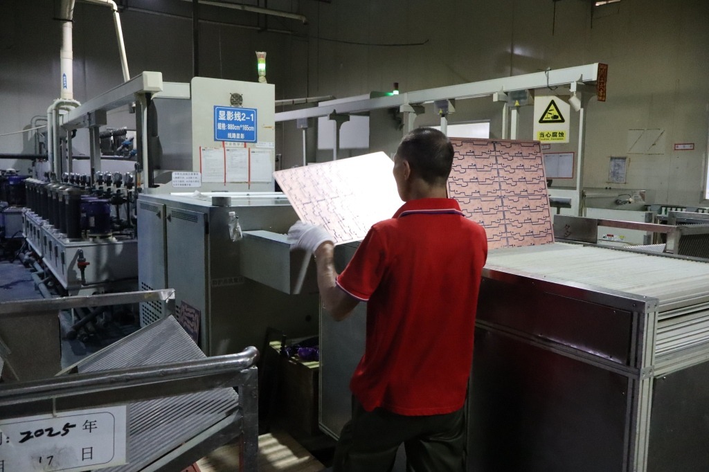
7. From Design Files to Physical Board: Manufacturing Reality
The manufacturing process looks straightforward on a slide deck. In practice, every step introduces variation.
It starts with laminate panels clad in copper. Images of the circuit are transferred, etched, drilled, plated, and laminated—sometimes multiple times. Each cycle adds tolerance stack‑ups. Drill wander of 75–100 microns doesn’t sound like much until annular rings get thin.
Solder mask alignment, surface finish choice (HASL, ENIG, OSP), and final routing all affect reliability. ENIG gives flat pads but brings black‑pad risk if the chemistry isn’t tightly controlled. HASL is robust and cheap, but uneven.
Assembly follows: paste, place, reflow. Lead‑free profiles push peak temps into the 240–250°C range. Boards not designed for that will warp. Some survive. Some don’t.
8. Common Circuit Board Failures and Practical Troubleshooting
Short circuits get all the attention, but they’re only part of the picture. Opens—often from cracked vias or lifted pads—are just as common and harder to spot.
Thermal issues show up subtly. A board passes at room temperature, fails at 70–80°C. IR imaging might show a hotspot running 28–34°C above ambient near a regulator or MOSFET. The fix isn’t always a heatsink; sometimes it’s copper distribution or via placement.
Mechanical stress causes quite a lot of damage. Flexing during installation can crack ceramic capacitors. Vibration loosens connectors. These failures show up weeks later, which is why they’re misdiagnosed.
Effective troubleshooting is systematic. Visual inspection, continuity checks, thermal probing, and then deeper electrical testing. Shops doing serious circuit board repair know that replacing components blindly wastes time. Understand the board—and the board usually tells you what went wrong.
9. Legislation, Compliance, and the Stuff Engineers Ignore Until a Shipment Gets Blocked
The fastest way to learn about electronics legislation is to violate it by accident. I’ve watched perfectly functional boards sit in a warehouse because someone ignored RoHS lead limits or didn’t think about WEEE labeling. The board worked. The paperwork didn’t. Guess which one mattered to customs.
For most commercial electronics, compliance boils down to a few repeat offenders: RoHS, REACH, and—if you’re unlucky—conflict minerals reporting. None of these changes how your circuit behaves electrically, but they absolutely affect material selection. Lead-free solder pushed reflow temperatures up into the 245–250°C range, which is why low-Tg laminates quietly disappeared from serious production years ago. If your printed circuit board can’t survive those temps without delamination, it’s dead on arrival.
Then there’s safety and flammability. UL94 V‑0 isn’t marketing fluff; it’s the difference between a pass and a recall when something overheats. In regulated sectors, IPC‑6012 Class 2 is usually the baseline, while Class 3 shows up where failure isn’t tolerated. I’m biased toward designing to Class 2+ margins even when the product spec doesn’t demand it. Boards don’t fail in neat, controlled lab conditions—they fail in basements, factories, and hot enclosures.
One more reality check: legislation changes more slowly than technology, but faster than most design cycles. Lock in materials early, confirm declarations from your fabricator, and keep documentation tied to the board revision. Fixing compliance after release costs more than fixing layout mistakes.
10. Technical Information That Actually Matters (Not the Datasheet Highlights)
Here’s a comparison I keep scribbled on whiteboards when teams argue about board specs. Not exhaustive—just the stuff that moves the needle in real builds.
| Parameter | Typical Range | Why You Should Care |
|---|---|---|
| Laminate Tg | 130–180°C | Below 150°C risks delamination with lead-free reflow |
| Copper Weight | 1–3 oz/ft² | Current capacity vs. etching tolerance trade-off |
| Trace/Space | 0.1–0.15 mm typical | Yield drops fast below most fab limits |
| Via Aspect Ratio | 6:1–10:1 | Higher ratios crack during thermal cycling |
People love obsessing over exotic parameters while ignoring basics like copper balance or solder mask clearance. That’s backwards. A boring FR‑4 board with good stackup discipline will outperform a fancy laminate laid out carelessly. I’ve seen it repeatedly.
Process capability matters as much as design intent. Not every shop can hit 0.1 mm spacing consistently, and pretending otherwise just creates yield problems. This is where talking to your fabricator early pays off. Shops like WellCircuits tend to be upfront about realistic limits, which saves everyone time.
11. Maintenance, Cleaning, and Why “Circuit Board Cleaner” Isn’t Magic
Here’s a common mistake: spraying half a can of solvent on a failing board and calling it maintenance. Cleaning helps, but only when contamination is the actual problem. Flux residue, conductive dust, and moisture paths—those respond well to proper cleaning. Cracked vias don’t.
Isopropyl alcohol in the 90%+ range handles most field work. Dedicated circuit board cleaner sprays evaporate faster and leave fewer residues, but they won’t fix corrosion that’s already eaten copper. I’ve opened boards where cleaning made things worse by pushing debris under fine‑pitch packages.
Preventive maintenance is mostly environmental control. Keep humidity reasonable, avoid condensation cycles, and don’t let boards bake in enclosures at 80–90°C continuously. That’s how solder joints fatigue early. In repair shops—what some people call “circuit board medics”—the first question isn’t “what cleaner?” but “why did this board need cleaning at all?”
Short version: clean gently, diagnose honestly, and stop expecting solvents to perform miracles.
12. When Things Fail: Repair vs. Redesign Isn’t an Emotional Decision
Search traffic for “circuit board repair near me” spikes every time a product hits end‑of‑life. That tells you something. Repair makes sense when failures are localized—burned regulators, lifted pads, worn connectors. It’s a bad idea when the root cause is structural.
Thermal damage, repeated via cracking, or widespread delamination usually point back to circuit board design choices. Fixing one board doesn’t fix the fleet. I’ve seen teams repair 20 units only to scrap the next 200 because the laminate couldn’t handle real operating conditions.
Redesign costs more upfront but less over time. Even small changes—thicker copper pours, relaxed trace spacing, better via stitching—can push lifetime from months to years. Repair is a bridge, not a destination.
If you’re maintaining legacy equipment, document every repair. Patterns emerge quickly, and those patterns tell you whether you’re fighting symptoms or causes.
13. How to Make a Circuit Board at Home (And Why It Teaches Humility)
DIY etching is where theory meets chemistry and usually loses the first round. The blue‑green liquid left after etching copper isn’t just ugly—it’s copper salts, and they’re toxic. Neutralization with baking soda until fizzing stops is common practice, but disposal rules vary. Don’t pour it down the drain and hope for the best.
Home processes teach valuable lessons: trace undercutting, pinholes in resist, and inconsistent results. That frustration mirrors real manufacturing challenges at a smaller scale. The difference is volume and repeatability. A method that works once on the bench may fail 30% of the time over ten boards.
I like DIY builds for learning, not for production. They show why professional fabs invest in controlled chemistry and waste handling. Also, wear gloves and eye protection. Copper chemistry doesn’t care how confident you feel.
14. Transferring Designs to Copper: Where Most DIY Boards Go Sideways
Finger oil ruins more boards than bad artwork. Clean copper with acetone or alcohol, let it dry, and don’t touch it again. That sounds trivial until you watch a transfer lift halfway through etching.
Alignment matters more than beginners expect. Tape edges, prevent sliding, and check orientation twice. Double‑sided boards without registration holes are an exercise in patience. This is why even simple commercial boards rely on drilled tooling holes early in the process.
The lesson carries into professional work: surface prep and process discipline beat clever tricks. Skip either one and defects follow.
15. Etching, Final Thoughts, and Where This All Lands
Etching looks dramatic, but it’s the least interesting part of board fabrication. Control the chemistry, agitate gently, and stop the process once copper clears. Over‑etching narrows traces and weakens pads. Under‑etching leaves shorts. There’s no heroism in rushing.
Zooming back out, circuit boards succeed or fail on fundamentals. Material selection, layout discipline, and realistic manufacturing assumptions matter more than buzzwords. Whether you’re building a Bluetooth circuit board, a power bank circuit board, or teaching kids with a circuit bread board, the principles don’t change.
I’ll leave you with this bias: spend more time on the board and less on the bill of materials. Components can be swapped. A bad PCB lives forever. If you’re unsure, review your assumptions, check standards, and talk to more than one fabricator before locking things down. That’s how reliable electronic circuit boards get built—quietly, carefully, and without drama.
If there’s one takeaway, it’s that a circuit board is an engineering system of its own, not a passive backdrop for components. Material selection affects reflow survivability. Layout decisions quietly determine EMI margins and thermal headroom. Manufacturing steps introduce constraints that no schematic can fix later. Ignore any one of those, and the board will eventually remind you—usually at the worst possible time.
The practical next step is discipline, not heroics. Define your real constraints first: current levels, operating temperature, expected lifetime, and production volume. Then sanity‑check materials, stackups, and spacing rules against those needs instead of defaulting to whatever “usually works.” Build and test a small batch, tear one down after stress testing, and look for early warning signs like pad lift or via distortion. Do that upfront, and you’ll spend a lot less time repairing boards and a lot more time shipping hardware that behaves the same in the field as it did on the bench.
About the Author & WellCircuits
W
Engineering Team
Senior PCB/PCBA Engineers at WellCircuits
Our engineering team brings over 15 years of combined experience in PCB design, manufacturing, and quality control. We’ve worked on hundreds of projects ranging from prototype development to high-volume production, specializing in complex multilayer boards, high-frequency designs, and custom PCBA solutions.
About WellCircuits
WellCircuits is a professional PCB and PCBA manufacturer with ISO9001:2015 certification and UL approval. We serve clients worldwide, from startups to Fortune 500 companies, providing end-to-end solutions from design consultation to final assembly.
Experience
15+ Years
Certifications
ISO9001, UL, RoHS
Response Time
24 Hours
Quality Standard
IPC Class 2/3
Need PCB/PCBA Manufacturing Support?
Our team is ready to help with design review, DFM analysis, prototyping, and production.Get in Touch