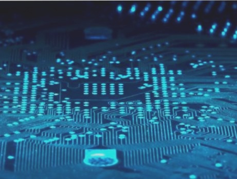
Understanding Printed Circuit Boards (PCBs)
A Printed Circuit Board (PCB) is a vital component in electronic devices, incorporating various complex processing technologies. PCBs can have different structures, such as single-layer, double-layer, or multi-layer, each requiring specific production methods.
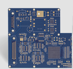
Components of a PCB
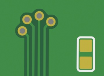
- Pad: Metal pads for soldering component pins.
- Via: Metal holes for interconnecting pins across layers.
- Mounting hole: Used for securing the PCB.
- Wire: Copper film connecting component pins.
- Connectors: Establish connections between PCBs.
- Filling: Copper coating to reduce impedance.
- Electrical boundary: Defines PCB dimensions.

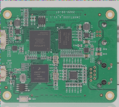
Types of PCB Layer Structures
- Single-layer board: Copper on one side, used for wiring and soldering.
- Double-layer board: Copper on both sides for component placement and soldering.
- Multilayer board: Multiple operational layers with various functions.
Working Layers in PCBs
- Signal layer: For component placement and wiring.
- Protective layer: Ensures specific areas remain untinned for reliability.
- Silk screen layer: Prints details like serial numbers and company names.
- Internal layer: Functions as a signal wiring layer.
- Other layers: Includes Drill Guide for indicating drilling hole locations.