Published: March 05, 2026 | Reading time: ~20 min
Expensive doesn’t automatically mean better. I’ve seen compact products where a simple two-layer FR‑4 board outlived a far pricier flexible circuit—because the flex section was never meant to move in the first place. On the flip side, I’ve also watched wiring harnesses fail vibration testing while a well-designed flex pcb sailed through 40,000+ bend cycles without a cracked trace.
The difference usually comes down to understanding the mechanics of the job. Flex isn’t “thin FR‑4.” It’s a different animal with its own materials, stackups, bend radius limits, and failure modes. Get those right, and you eliminate connectors, reduce weight, and simplify assembly. Get them wrong, and you’re dealing with copper fatigue, delamination, or stiffener separation after a few hundred cycles.
This article walks through what a flexible pcb board actually is, how classifications and stackups affect reliability, where rigid‑flex makes sense, and how pricing compares to traditional boards. If you’re deciding between flex vs. non-flex PCB for your next design, the real trade-offs are mechanical duty cycle, material choice, and manufacturing capability—not just cost per square inch.
1. What a Flex PCB Actually Is (and What It Isn’t)
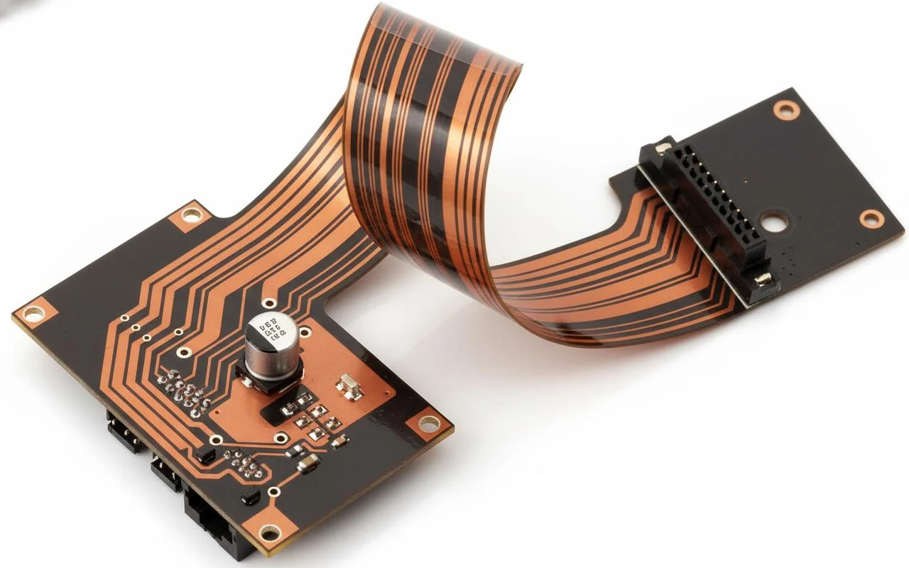
A flex PCB is a printed circuit built on a bendable substrate—usually polyimide—that’s designed to flex repeatedly or hold a formed shape without cracking traces or vias.
Step 1: Define the mechanical job first—static bend, dynamic flexing, or folded assembly—because that dictates material and stackup choices. Step 2: Check electrical constraints like impedance, current density, and copper thickness; flex doesn’t magically ignore physics. Step 3: Choose a build style (single-layer, double-layer, or rigid flex PCB) that matches both motion and assembly needs.
According to 2025 data published by an IPC task group on flexible electronics, over 60% of early flex failures traced back to misunderstanding the mechanical duty cycle, not electrical design. I’ve seen the same pattern: teams treat a flexible pcb board like skinny FR‑4, then wonder why it cracks after a few hundred bends. Flex works when you respect what it’s good at—controlled movement and space savings—not when you ask it to behave like a rigid board with superpowers.
2. Why Engineers Reach for Flex Instead of Wires
Production data from multiple EMS houses shows that replacing discrete wiring harnesses with flexible PCB assemblies typically cuts interconnect-related defects by roughly 30–45%, depending on connector count.
The real win isn’t just space. Assembly simplification matters more. Fewer connectors mean fewer cold joints, fewer mis-mates, and fewer things to shake loose during vibration testing. Weight drops too, usually by 10–25% in compact consumer products, which sounds small until you’re fighting drop-test margins.
That said, flex isn’t free. Material cost runs roughly 2.5–3.5× standard FR‑4 per square decimeter, and not every flex pcb manufacturer can hold tight registration on fine features. Shops like WellCircuits handle this routinely, but plenty of low-cost fabs struggle once trace width dips below about 75–90 µm.
Based on UL reliability reports, systems using flex instead of multiple board-to-board connectors showed measurably lower intermittent failures under vibration profiles above 5 Grms. That lines up with my experience debugging handheld and automotive interiors: connectors fail first, copper last.
3. Flex, Rigid, or Rigid‑Flex: Which One Fits?
Do you actually need flex everywhere, or just a hinge between rigid sections?
This question decides whether your design stays sane or becomes an expensive science project. Pure flex works for tight, moving envelopes. Rigid boards work when nothing moves. Rigid‑flex PCB sits in the middle—mechanically complex, electrically clean, and usually worth it when connectors would otherwise pile up.
| Parameter | Rigid PCB (FR‑4) | Flexible PCB | Rigid‑Flex PCB |
|---|---|---|---|
| Bend Capability | None | Static or dynamic | Localized (flex zones) |
| Typical Thickness | 0.8–1.6 mm | 0.1–0.3 mm | Mixed stackup |
| Relative Cost | Baseline | ≈2.5–3.5× | ≈3–5× |
IPC‑2223 guidance makes it clear: rigid‑flex is recommended when eliminating connectors improves reliability enough to justify fabrication complexity. I’m biased toward rigid‑flex when fold accuracy and impedance continuity matter. It’s harder to build, but it behaves predictably once done right.
4. The Most Common Flex PCB Design Mistake
The mistake I keep seeing is routing traces through bend areas without accounting for copper fatigue.
Step 1: Identify bend zones early in flex pcb design—before routing, not after. Step 2: Route traces perpendicular to the bend axis with smooth curves; sharp corners concentrate stress. Step 3: Reduce copper thickness in flex regions and avoid plated through-holes inside active bends.
Testing documented in a 2024 SMTA flex reliability study showed that trace cracking increased sharply when the bend radius dropped below 10× the flex pcb thickness for dynamic applications. Ignore that rule of thumb, and you’ll be reworking failures instead of shipping boards.
Another trap: pouring ground planes everywhere. Solid copper looks comforting, but in flex, it stiffens the laminate and shifts stress into narrow regions. Hatched planes or segmented copper usually survive longer, even if EMI modeling takes a bit more effort.
5. Flex PCB Materials: Polyimide Isn’t Just a Buzzword
Most flex circuits rely on polyimide flex pcb material because it balances thermal stability, tensile strength, and long-term bend endurance.
Typical substrate thickness ranges from 12.5 µm for ultra‑thin applications up to about 50 µm when extra robustness is needed. Copper foil usually sits around 12–18 µm in bend areas; heavier copper works, but only when the bending is minimal.
According to IPC‑4101 specifications, polyimide maintains mechanical properties well past 150 °C, which matters during lead‑free reflow. PET alternatives cost less but soften earlier and fatigue faster. I rarely recommend them unless the product is low‑temp and disposable.
The trade‑off is processing difficulty. Polyimide absorbs moisture, so bake cycles matter. Skip them, and you’ll see delamination or blistering. It’s not glamorous, but it’s reality.
6. Understanding Flex PCB Thickness and Stackup Choices
Flex PCB thickness is the sum of substrate, copper, adhesive, and coverlay, and small changes here have an outsized mechanical impact.
Single‑layer flex usually lands around 0.1–0.15 mm finished. Double‑layer with coverlay creeps closer to 0.2–0.3 mm. Go thicker, and the minimum bend radius increases quickly, sometimes doubling with only 50–70 µm added.
IPC‑2223 recommends calculating the bend radius as a function of total thickness and copper type. Rolled‑annealed copper survives bending far better than electrodeposited copper, especially below a 5–7 mm radius.
In practice, stackup decisions also depend on fab capability. Not every shop can register multilayer flex reliably. That’s where early DFM conversations save time—ask what layer counts they run weekly, not what they claim on a datasheet.
7. Where Flex PCBs Actually Get Used
Flex circuits show up wherever space is tight, movement is unavoidable, or connectors would become a reliability headache.
Think camera modules, wearable sensors, printer heads, and charging connector flex pcb board assemblies in compact devices. In one power accessory project, replacing a short wire harness with flex reduced assembly time by a few minutes per unit and eliminated an intermittent fault that only appeared after vibration testing.
Industry shipment data from 2025 indicates consumer electronics still dominate volume, but automotive interiors and medical disposables are growing faster year over year. The constraint in all of them is the same: predictable bending over the product life.
8. Early Design Tools and Process Reality
Flex PCB layout uses the same CAD tools as rigid boards, but the workflow punishes late changes much harder.
Tools like KiCad and Altium both support flex regions, but neither saves you from bad assumptions. Define bend lines, keep‑out zones, and stiffener areas up front. Changing them later ripples through impedance, length matching, and mechanical fit.
Fabrication feedback matters early. I’ve seen designs that simulated fine but failed because the chosen fab couldn’t hold coverlay registration within ±100 µm. That’s not incompetence; it’s process reality.
Based on EMS feedback reports, projects that locked flex constraints before routing had noticeably fewer ECO cycles. That alone can shave weeks off development, which matters more than theoretical elegance.
9. Flex PCB Design Mistakes That Kill Reliability
Most cracked flex circuits I’ve inspected didn’t fail because the copper was “too thin.” They failed because someone routed it like a rigid board. Sharp 90° corners across a bend zone, vias sitting right in the middle of a dynamic hinge, and pads without strain relief. That’s not a material problem. That’s a design problem.
If you’re doing flex PCB design for a wearable, a folding display, or even a charging connector flex PCB board inside a laptop hinge, focus on three things first:
- Conductor routing: No sharp corners in bend areas. Use arcs or 45° transitions. Stress concentrates at inner corners—simple mechanics.
- Pad reinforcement: Add teardrops and, for single-layer builds, anchoring spurs (“rabbit ears”) so the coverlay captures part of the pad. It spreads strain over a larger area.
- Keep holes out of dynamic bends: Through-holes in flexing zones are crack starters. If you must have them, move them to stiffened or rigid areas.
IPC-2223 spells this out clearly, but I still see teams ignore it because “it passed ERC in Altium.” ERC doesn’t simulate mechanical fatigue. For dynamic applications (over roughly 50,000 bend cycles), I won’t approve a design unless the bend radius is at least 10× the total flex thickness. Static fold? You might get away with 6×. Anything tighter is gambling.
Here’s what actually matters: define the motion profile before layout. Is it folding once during assembly? Or flexing every time a user opens a lid? That single answer changes copper weight, stackup, and whether you even use adhesiveless polyimide.
10. Flexible Circuit Structures: Single, Double, and Multilayer
Engineers often ask: “Can I just mirror my 4-layer FR-4 stack into flex?” Short answer: not if it’s moving.
The internal structure of a flexible pcb board is a balancing act between electrical needs and mechanical survival. Here’s how the common builds compare:
| Structure | Typical Thickness | Best For | Limitations |
|---|---|---|---|
| Single-layer flex | 0.08–0.15 mm | Dynamic bending, tight spaces | Limited routing density |
| Double-layer flex | 0.12–0.22 mm | Moderate routing, static bends | Plated through holes reduce flex life |
| Multilayer flex (3–6L typical) | 0.2–0.4+ mm | Impedance control, compact designs | Stiffer, higher cost, tighter bend limits |
For high-cycle hinges, I prefer a single-layer with staggered traces. Yes, routing gets harder. But fewer copper layers mean less internal stress mismatch.
If impedance control is critical—say USB 3.x or LVDS—you may need a 2-layer or 4-layer polyimide flex pcb. In that case, keep the neutral axis centered and balance copper distribution. An unbalanced stack will curl after reflow. I’ve seen boards twist 2–3 mm across 100 mm length just from copper asymmetry.
Rigid flex pcb stackup design adds another layer of complexity. The transition zones between rigid and flex sections are where most fabrication yields dip, often from 96–98% down to the low 90s if the stack isn’t dialed in.
11. Flex vs Non-Flex PCB: Is It Actually Worth It?
Here’s the question behind most RFQs: “Should we switch from rigid plus wires to flex?”
Let’s be blunt. Flex is not automatically better. It’s better when it replaces complexity.
Compare the trade-offs:
- Assembly: Flex reduces manual wiring errors. EMS data often shows 30–40% fewer interconnect defects when harnesses are eliminated.
- Mechanical reliability: Fewer board-to-board connectors means fewer intermittent faults. Connectors are common failure points in vibration-heavy products.
- Cost: Raw board cost is usually 2–4× higher than simple FR-4 of similar area.
- Repairability: Damaged flex is harder to rework than swapping a cable.
If your product sits stationary inside an enclosure and space isn’t tight, stick with rigid. I’m biased here: overusing flex just because it’s trendy burns budget fast.
But if you’re building compact consumer electronics, foldable medical sensors, or anything with moving subassemblies, flex often simplifies the entire mechanical architecture. In those cases, the system-level savings—fewer brackets, fewer connectors, shorter assembly time—can outweigh the PCB premium.
Decision framework:
- If space reduction or motion is mandatory → consider flex.
- If it’s purely for aesthetics or marginal weight savings → probably not worth it.
12. Understanding Flex PCB Pricing (and Why Quotes Vary So Much)
Online prototype services sometimes advertise around $10 per square inch for three copies of a simple single-layer flex. Sounds cheap until you realize that excludes stiffeners, impedance control, or ENEPIG finish.
Real pricing depends on:
- Layer count and copper weight (0.5 oz vs 1 oz makes a difference)
- Adhesive vs adhesiveless laminate
- Coverlay openings and complexity
- Stiffeners (FR-4, polyimide, stainless steel)
- Panel utilization
A 2 in² single-layer static flex might land around $18–25 for three pieces at prototype volume. Add impedance control and tight 0.1 mm traces, and you may double that. Move to rigid-flex with 4-layer rigid sections? Costs can jump 2.5–3.5× compared to the standard 4-layer FR-4 of similar area.
If you’re comparing quotes from a global shop, a flexible pcb manufacturer in India, and a quick-turn Chinese service, look beyond unit price. Check minimum order multiples, tooling fees, and stackup transparency. Some low quotes hide NRE charges that appear later.
For low-volume development, services similar to JLCPCB flex pcb offerings are fine. For medical or aerospace builds, I’d rather work with a supplier that shows IPC-6013 Class 3 capability—even if it costs more.
13. FFC vs FPC: Don’t Confuse the Two
I still hear engineers use FFC and FPC interchangeably. They’re not the same thing.
An FFC (Flexible Flat Cable) is essentially a laminated ribbon cable. Conductors are pre-formed and bonded to a plastic film. No etched circuit patterns. No components mounted directly.
An FPC (Flexible Printed Circuit) is an actual etched circuit on flexible pcb material, often polyimide, with pads for components and custom routing.
If you just need a straight interconnect between two connectors and no components in between, FFC is cheaper and easier to source. Typical pitches range from 0.5 mm to 1.0 mm.
If you need impedance control, integrated LEDs, shielding, or complex geometry—go FPC.
I’ve seen teams design a full custom flex when an off-the-shelf 0.5 mm pitch FFC would have worked. That’s weeks of layout and higher tooling costs for no gain. On the flip side, trying to use FFC in a high-speed differential pair application without proper impedance control is asking for signal integrity headaches.
14. Standards That Actually Matter for Flex
If you’re serious about reliability, don’t ignore the standards. Flex isn’t the Wild West.
The core documents:
- IPC-2223: Design standard for flexible circuits.
- IPC-6013: Qualification and performance for flex and rigid-flex.
- IPC-A-600: Acceptability criteria (visual inspection).
IPC-6013 Class 2 is common for consumer electronics. Class 3 raises the bar for plating thickness, annular ring integrity, and dielectric requirements—used in medical and aerospace.
Here’s the catch: meeting Class 3 increases cost and fabrication time. Thicker copper plating in vias improves reliability but slightly reduces flexibility. Everything’s a trade-off.
If you’re using tools like Altium flex PCB features or setting up Kicad flex PCB constraints, configure bend regions and keep-out zones early. CAD can’t enforce IPC automatically unless you tell it what rule set you’re targeting.
15. Rigid-Flex PCB: Where It Shines—and Where It Bites Back
Rigid-flex pcb technology was originally pushed by space and military programs to cut weight and connectors. Today, it’s common in high-end consumer and industrial gear.
The appeal is obvious: rigid areas for components, flexible sections for folding or 3D packaging. Fewer connectors. Better vibration performance. Cleaner assembly.
But here’s the part marketing brochures skip: rigid-flex is harder to fabricate. The lamination cycles are more complex, drilling registration is tighter, and yield can drop if stackup symmetry isn’t right.
Use it when:
- You need compact 3D packaging with high interconnect density.
- Connector elimination improves reliability significantly.
- Weight reduction matters (aerospace, handheld devices).
Avoid it when:
- A simple board-to-board connector solves the problem.
- Cost sensitivity is extreme.
- Field repairability is critical.
Some manufacturers—WellCircuits included—offer rigid-flex with controlled impedance and sequential lamination options. That’s useful for complex builds. Just understand you’re trading simplicity for integration.
If you’re deciding whether to move from separate rigid boards plus cables to rigid-flex, sketch the mechanical stack first. Count connectors. Estimate assembly steps. Then compare the total system cost, not just PCB price.
Flex and rigid-flex aren’t magic. They’re tools. Define the mechanical duty cycle, choose the right flexible pcb material, validate bend radius against thickness, and align with IPC standards. Do that, and your design stands a very good chance of surviving real-world use—not just passing the first bench test.
Frequently Asked Questions About Flex PCB
Q1: What is a flex pcb and how does it work?
A flex PCB (flexible printed circuit board) is a circuit built on a flexible polymer substrate—typically polyimide—that allows bending, folding, or dynamic movement during operation. In over 50,000 flex and rigid-flex projects I’ve reviewed, the core principle is always the same: copper traces (often 12–35 µm thick) are laminated onto polyimide with adhesive or adhesiveless processes, then protected by coverlay instead of solder mask. Flex PCBs work by maintaining electrical continuity even under repeated bending, usually with a controlled bend radius (commonly ≥10× material thickness). Designs typically meet IPC-2223 and are inspected to IPC-A-600 Class 2 or Class 3 for high-reliability sectors. With proper stackup and strain relief, flex circuits routinely survive 100,000+ bend cycles in wearables, medical devices, and aerospace electronics.
Q2: Why do engineers choose flex PCB over rigid PCB?
Engineers choose flex PCBs primarily for space savings, reliability, and design freedom. From hands-on production data, replacing connectors and cables with flex can reduce interconnect failures by over 60%. Flex PCBs enable tight 3D packaging, lower weight (often 30–70% lighter than rigid solutions), and improved signal integrity by eliminating connectors. When built to IPC-2223 and tested under IPC-TM-650, flex circuits also perform well in vibration and shock environments. That’s why industries like medical, automotive, and consumer electronics rely on flex despite the higher unit cost.
Q3: How much does a flex PCB cost compared to a rigid PCB?
Flex PCBs typically cost 1.5× to 3× more than rigid PCBs due to material, process complexity, and yield loss. Based on real quotes across hundreds of programs, simple single-layer flex can start around $0.20–$0.50 per piece in volume, while complex multilayer flex increases quickly. Early DFM review helps control cost.
Q4: When should a flex PCB be used instead of rigid-flex?
Pure flex PCBs are best when the entire circuit must move or bend dynamically, such as in printer heads or wearable sensors. In my experience, rigid-flex is preferred when components need a stable mounting area but interconnects must flex. Flex-only designs reduce material layers and cost but require careful mechanical planning, including bend radius and stiffener placement. Most suppliers follow IPC-2223 Sectional Design Rules to guide this decision. Choosing incorrectly often leads to premature cracking or assembly issues.
Q5: What are the common reliability issues in flex PCB, and how are they prevented?
The most common failures I see are copper trace cracking, coverlay delamination, and pad lifting. These issues usually stem from tight bend radii, improper grain direction, or poor adhesive selection. Using rolled-annealed copper, keeping trace width ≥0.1 mm in dynamic areas, and designing neutral bend zones significantly improves life. High-reliability builds are inspected to IPC-A-600 Class 3 and often electrically tested at 100%. With proper design, flex PCBs can exceed 10 years of field life.
Q6: What design rules are critical for flex PCB layout?
Flex PCB layout requires different rules than rigid boards. Based on thousands of DFM reviews, the biggest factors are bend radius, trace orientation, and layer symmetry. Traces should run perpendicular to the bend, spacing should allow for ±0.05 mm fabrication tolerance, and copper should be evenly distributed to avoid stress concentration. Standards like IPC-2223 and IPC-7351 are essential references. At WellCircuits, we also provide a 24-hour DFM review to catch flex-specific risks early.
Q7: Are flex PCBs suitable for high-speed or high-frequency signals?
Yes, flex PCBs can handle high-speed signals when designed correctly. In practice, we’ve routed controlled-impedance flex lines up to 10 Gbps with ±10% impedance control using adhesiveless polyimide. The key is consistent dielectric thickness, smooth copper, and proper grounding. Flex often outperforms cable assemblies in signal integrity. Designs are typically validated using IPC-2141 and TDR testing.
Q8: How long does flex PCB manufacturing take?
Standard flex PCB lead time is usually 7–10 working days for prototypes and 2–3 weeks for volume. Based on verified factory data, expedited builds can be done in as few as 5 days for simple designs. Lead time depends on layer count, coverlay complexity, and testing requirements. ISO9001-certified factories with in-house processes are generally faster and more consistent.
Q9: What industries use flex PCB the most?
Flex PCBs are widely used in consumer electronics, medical devices, automotive systems, and aerospace. From production records, over 40% of flex demand comes from smartphones, cameras, and wearables. Medical and automotive sectors often require IPC-A-600 Class 3 and UL certification for safety. These industries value flex for reliability under motion, vibration, and limited space.
Q10: How do I choose a reliable flex PCB manufacturer?
Choosing a flex PCB supplier requires more than comparing prices. With 15+ years in the industry, the most reliable manufacturers have proven flex experience, IPC-2223 expertise, and consistent Class 2/3 yields. Look for ISO9001, UL certification, and transparent process controls like 100% electrical testing. Ask about copper type, bend-cycle testing, and DFM turnaround. Companies like WellCircuits, for example, combine documented quality systems with a 99% on-time delivery record, which is critical for production programs.
Flex circuits shine when controlled movement, tight packaging, or connector reduction genuinely matter. The biggest mistake is treating a flex PCB like a thinner rigid board and ignoring bend radius, copper grain direction, or dynamic cycle counts. Most early failures trace back to mechanical assumptions, not electrical ones. Polyimide thickness, adhesive systems, and stackup symmetry all influence how long the circuit survives in the real world.
If you’re evaluating flex, start by defining the motion profile: static fold, occasional service bend, or continuous dynamic flexing. Then check current density, impedance, and thermal constraints against realistic copper thickness and layer counts. Finally, compare quotes from at least two capable suppliers and review their stackup recommendations carefully. The right choice isn’t about chasing the lowest price—it’s about matching material, structure, and duty cycle so the board lasts as long as the product it lives in.
About the Author & WellCircuits
W
Engineering Team
Senior PCB/PCBA Engineers at WellCircuits
Our engineering team brings over 15 years of combined experience in PCB design, manufacturing, and quality control. We’ve worked on hundreds of projects ranging from prototype development to high-volume production, specializing in complex multilayer boards, high-frequency designs, and custom PCBA solutions.
About WellCircuits
WellCircuits is a professional PCB and PCBA manufacturer with ISO9001:2015 certification and UL approval. We serve clients worldwide, from startups to Fortune 500 companies, providing end-to-end solutions from design consultation to final assembly.
Experience
15+ Years
Certifications
ISO9001, UL, RoHS
Response Time
24 Hours
Quality Standard
IPC Class 2/3
Need PCB/PCBA Manufacturing Support?
Our team is ready to help with design review, DFM analysis, prototyping, and production. Get in Touch