Understanding the PCB Fabrication Process: A Comprehensive Guide for Electronics Manufacturers

What Is a Printed Circuit Board (PCB)?
A Printed Circuit Board (PCB) serves as the foundation for most modern electronic devices, providing both electrical connectivity and mechanical support for components. These essential boards power everything from smartphones and laptops to industrial automation systems and medical equipment. As global demand for high-quality PCB manufacturing grows, understanding the fabrication process becomes crucial for businesses sourcing reliable PCB suppliers in China.
Key Applications of PCBs in Modern Electronics
- Consumer electronics (smartphones, tablets, smart home devices)
- Computing hardware (motherboards, GPUs, servers)
- Industrial automation systems
- Medical diagnostic equipment
- Automotive electronics and IoT devices
PCB Types: Choosing the Right Board for Your Application
When selecting a PCB manufacturer in China for your export business, consider these four primary board types:
- Single-sided PCBs – Cost-effective for simple circuits
- Double-sided PCBs – Enhanced circuit density for mid-range applications
- Multi-layer PCBs – Ideal for complex, high-performance electronics
- Flexible PCBs – Specialized solutions for space-constrained applications
The Complete PCB Fabrication Process: Step-by-Step
1. Design Review and Preparation
Before beginning PCB fabrication for export, conduct a thorough engineering review. This includes:
- Verifying circuit schematics and component placement
- Confirming design rule compliance (DRC)
- Validating material specifications for international standards
2. Core Manufacturing Steps
Lamination Process
The fabrication begins with applying dry film to copper laminate boards, followed by direct laser imaging to create circuit patterns. After UV exposure and development:
- Inner layers undergo oxide treatment for improved bonding
- Pre-preg and copper foil layers are alternated
- Hydraulic pressing creates the final “PCB sandwich” structure

Precision Drilling
Specialized equipment drills micro-vias for layer interconnection:
- Holes are typically 5 mils larger than final specifications
- Copper plating ensures proper electrical connectivity
- Supports high-density interconnect (HDI) PCB manufacturing
Copper Deposition and Electroplating
“The copper plating process is critical for ensuring signal integrity in multi-layer PCBs. Our Shenzhen-based PCB factory uses advanced electroplating baths with precise current control for consistent results.”
Final Finishing
The completed board receives:
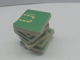
- Solder mask application (typically green for optimal inspection)
- Silkscreen printing for component identification
- Surface finish (HASL, ENIG, or immersion silver)
Quality Assurance in PCB Manufacturing
Reputable PCB manufacturers in China implement rigorous testing protocols:
- Automated Optical Inspection (AOI)
- Electrical testing (flying probe or fixture-based)
- Microsection analysis for multilayer verification
- Environmental stress testing for export-quality boards
Why Choose Professional PCB Fabrication Services?
For businesses requiring high-quality PCB assembly for export, professional fabrication offers:
- Consistent quality through controlled processes
- Cost efficiency at production scale
- Technical expertise in material selection and DFM
- Regulatory compliance for international markets
Partner with a Trusted PCB Manufacturer
Shenzhen WellCircuits Technology Co., Ltd. specializes in high-mix, low-volume PCB production with quick turnaround times. Our comprehensive services include:
- PCB design and engineering support
- Prototype to volume production
- Component sourcing and procurement
- Complete box-build assembly
- Quality testing and certification
For businesses seeking reliable PCB fabrication in China, our expertise ensures your electronic products meet the highest international standards. Contact us today to discuss your project requirements.