PCB Design and Layout: The Foundation of Modern Electronics Manufacturing

What Is PCB Design and Why It Matters in Global Electronics Trade
PCB (Printed Circuit Board) design represents the critical first step in developing reliable electronic products for international markets. As leading PCB manufacturers in China and worldwide continue innovating, understanding proper PCB layout principles becomes essential for import/export businesses sourcing electronic components.
“Proper PCB design reduces manufacturing costs by 30-40% while improving product reliability – a crucial advantage in competitive global markets.”
The Anatomy of a High-Quality PCB: Layer by Layer Breakdown
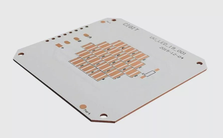
1. Silkscreen Layer: The Identification System
The white markings on PCBs serve vital functions for electronics assembly and troubleshooting. This layer helps:
- Identify components and polarity
- Mark test points and connectors
- Display manufacturer information and certifications
2. Solder Mask: The Protective Shield
This iconic green coating (available in multiple colors) provides:
- Insulation between copper traces
- Oxidation protection
- Soldering guidance during PCB assembly
3. Copper Layer: The Conductive Pathway
The conductive foundation comes in different weights:
- Standard 1oz/sq ft (35μm) for most applications
- 2oz/sq ft for high-current designs
- Heavy copper (3oz+) for power electronics
4. FR4 Substrate: The Structural Core
This fiberglass-reinforced epoxy laminate offers:
- Excellent mechanical stability
- High temperature resistance
- Consistent dielectric properties

Best Practices for PCB Design and Layout in Export Manufacturing
Step 1: Define Product Requirements
Successful PCB design for export begins with understanding:
- Operating environment (temperature, humidity, vibration)
- Certification requirements (CE, UL, RoHS)
- Target manufacturing processes
Step 2: Schematic Capture
Create comprehensive documentation including:
- Component specifications
- Netlist connections
- Design constraints
Step 3: Component Placement Strategy
Optimize for both function and manufacturability:
- Group related components
- Consider thermal management
- Plan for automated assembly
Step 4: Intelligent Routing
Implement professional routing techniques:
- Maintain proper trace spacing
- Optimize signal integrity
- Minimize EMI issues
Step 5: Design Verification
Critical checks before manufacturing:
- Design rule check (DRC)
- Electrical rule check (ERC)
- 3D mechanical verification
8 Critical Factors for Export-Quality PCB Designs
- Manufacturing Process Compatibility – Match design to production capabilities
- Board Size Optimization – Balance functionality and cost
- Material Selection – Choose appropriate substrate and finishes
- Component Sourcing – Verify global availability
- Thermal Considerations – Plan for heat dissipation
- Testability – Include test points for quality control
- Design for Assembly – Facilitate efficient production
- Documentation – Provide complete manufacturing files
Why Partner with Professional PCB Manufacturers for Export?
Working with experienced PCB suppliers in China offers significant advantages:
- Access to advanced manufacturing technologies
- Cost-effective production at scale
- Compliance with international standards
- Reliable supply chain management
- Technical support throughout product lifecycle
Conclusion: PCB Design as a Competitive Advantage
Mastering PCB layout and design principles provides exporters with:
- Faster time-to-market
- Higher product reliability
- Lower manufacturing costs
- Better quality control
By implementing professional PCB design practices, businesses can develop competitive electronic products for global markets while maintaining efficient, cost-effective manufacturing processes.