What Is Lead-Free Solder? A Manufacturing Engineer’s Complete Guide
Lead-free solder is a tin-based alloy — most commonly SAC305, a composition of 96.5% tin, 3% silver, and 0.5% copper — that replaced traditional tin-lead formulations in commercial electronics assembly following the EU RoHS Directive in July 2006. It melts at approximately 217°C and requires reflow oven peak temperatures of 245-260°C to achieve reliable wetting and joint formation. For anyone specifying materials for a new product, qualifying a contract manufacturer, or managing a transition from tin-lead, this guide covers every dimension that affects a manufacturing outcome: alloy selection, reflow profiling, reliability trade-offs, IPC compliance, and the process changes that make or break a transition.
TL;DR / Key Takeaways
- Lead-free solder is any solder alloy without lead; the global commercial standard is SAC305 (96.5Sn/3Ag/0.5Cu) with a liquidus of 217°C and a recommended reflow peak of 245-260°C
- The EU RoHS Directive (2002/95/EC, effective July 2006) mandated lead-free for consumer electronics sold in Europe; China RoHS, Japan JIS C 0950, and US state-level rules followed
- Reflow temperatures are 30-40°C higher than tin-lead, which stresses PCB substrates, accelerates pad oxidation, and reduces the process window
- Drop shock resistance is the primary trade-off — BGA and QFN joints in consumer electronics are most vulnerable
- Tin whisker growth on pure-tin finished components increased after lead removal; mitigation strategies include alloying, reflow conversion, and conformal coating
- Transitioning requires process recipe changes, not material substitution alone — operators trained on tin-lead technique will produce cold joints on lead-free without retraining
- IPC J-STD-001 governs workmanship standards for lead-free assembly; demand third-party certification from your contract manufacturer
Table of Contents
- What Is Lead-Free Solder?
- Why Lead Was Removed From Solder
- Lead-Free Solder Alloys: Beyond SAC305
- The Lead-Free Reflow Profile
- Lead-Free Solder vs Leaded: The Real Trade-offs
- IPC Standards for Lead-Free Assembly
- How to Transition From Tin-Lead to Lead-Free
- Why Lead-Free Solder Matters for Your PCB Project
- Frequently Asked Questions
- Related Guides
What Is Lead-Free Solder?
Lead-free solder is a family of alloys used to join electronic components to printed circuit boards without the toxicity of lead. The most widely adopted composition worldwide is SAC305, shorthand for 96.5% tin (Sn), 3.0% silver (Ag), and 0.5% copper (Cu). SAC305 has a solidus temperature of 217°C and a liquidus of 220°C — the 3°C gap between them is narrow enough that the alloy behaves nearly as a single melting-point material, which simplifies reflow oven profiling compared to multi-phase solders with broader melting ranges.
In practical assembly terms, the reflow oven needs to hit a peak temperature of 245-260°C to reliably wet all joints on a standard SAC305 assembly run. For tin-lead 63/37 solder, the equivalent peak is 225-235°C. That 20-30°C difference sounds manageable on paper. In a production environment, it is the difference between a forgiving process window and a tight one. The higher temperature stresses PCB substrates, accelerates oxidation on component leads and PCB pads, and gives operators a narrower margin before wetting fails.
**What most buyers overlook is that "lead-free solder" is not a single material.** There are meaningful performance differences between SAC305, SAC387, SAC405, SACM, Sn99.3Cu0.7, and the bismuth-based alloys used in thermal-sensitive applications. If a component datasheet or BOM says "lead-free solder," ask for the specific alloy designation — because the category covers a wide performance range, and not all lead-free alloys are interchangeable.
Why Lead Was Removed From Solder
Tin-lead solder — historically 63/37 eutectic tin-lead — was the standard for electronics assembly for over 50 years. It performed well: a low melting point of 183°C, fast wetting, reliable joint formation, and a forgiving process window. The problem was not performance. It was toxicity.
Lead is a neurotoxin that accumulates in the body through repeated occupational exposure. Workers in electronics manufacturing facilities who handle lead-bearing solders face documented health risks from lead fumes and lead-contaminated surfaces. Beyond the workplace, end-of-life electronics in landfills present an environmental contamination pathway — lead can leach into groundwater and soil.
The regulatory response came from the European Union. The RoHS Directive (Restriction of Hazardous Substances in Electrical and Electronic Equipment, 2002/95/EC, effective July 2006) banned lead and five other substances — cadmium, mercury, hexavalent chromium, polybrominated biphenyls (PBBs), and polybrominated diphenyl ethers (PBDEs) — in ten categories of consumer electronics sold in EU markets. China followed with China RoHS (2006), Japan with JIS C 0950 (2008), and several US states enacted similar requirements, most notably California’s RoHS law.
The EU RoHS exemptions have narrowed over successive recasts. The original 2006 mandate covered ten product categories. RoHS 2 (Directive 2011/65/EU) expanded scope and introduced conformity assessment procedures. RoHS 3 (Delegated Directive (EU) 2015/863) added four phthalate plasticizers to the restricted substance list. The result is a progressively tighter regulatory framework that now covers nearly all electrical and electronic equipment placed on the EU market.
**What the transition actually cost the industry is underreported.** When RoHS took effect in 2006, the electronics industry spent an estimated 10-15 years in active transition — re-qualifying thousands of component part numbers for higher reflow temperatures, retraining assembly technicians, and re-qualifying solder paste formulations. The process knowledge gaps from that transition are still visible in field failure data from products manufactured between 2006 and 2015, when the industry was still learning to optimize lead-free reflow profiles for commercial-scale production.
Lead-Free Solder Alloys: Beyond SAC305
SAC305 is the global workhorse, but it is not the only option. Different applications call for different alloys — some prioritizing mechanical shock resistance, others optimizing for thermal cycling or cost.
Common Lead-Free Solder Alloys
| Alloy | Composition | Melting Range | Primary Application |
|---|---|---|---|
| **SAC305** | 96.5Sn/3Ag/0.5Cu | 217-220°C | General SMT, BGA, QFN — the global standard |
| **SAC387** | 95.5Sn/3.8Ag/0.7Cu | 217-227°C | Higher silver for improved wetting |
| **SAC405** | 95.5Sn/4Ag/0.5Cu | 217-227°C | QFN and fine-pitch components |
| **SACM** | 98.3Sn/0.7Ag/0.5Cu/0.1Sb | 221-226°C | Modified formulation for reduced tin whisker growth |
| **Sn99.3Cu0.7** | 99.3Sn/0.7Cu | 227°C | Wave soldering, cost-sensitive applications |
| **Sn96Ag4** | 96Sn/4Ag | 221-236°C | Die-attach, specialty applications |
| **Sn42Bi58** | 42Sn/58Bi | 138°C | Low-temperature assembly, thermally sensitive components |
**No lead-free alloy matches tin-lead on every dimension.** SAC305 is the best all-around compromise for most SMT assembly, but it has two genuine weaknesses: drop shock resistance and sensitivity to fine-pitch component behavior. For consumer wearables and mobile electronics where drop survival is a specified requirement, Sn-Ag-Bi alloys or modified SAC compositions with minor nickel, germanium, or rare earth additions offer measurably better mechanical resilience under impact loading. The tradeoff is typically higher material cost and more demanding process requirements.
Tin Whiskers: The Problem Lead Suppressed
One of the most consequential reliability concerns with lead-free solder — particularly with pure-tin finished components — is tin whisker growth. Tin whiskers are conductive crystalline filaments that spontaneously grow from tin surfaces, sometimes years after manufacture. They can reach lengths sufficient to bridge adjacent component leads or traces, creating short circuits in finished assemblies.
Lead suppresses tin whisker growth by modifying the grain boundary structure of the solder joint. This is why tin-lead solder had virtually no documented whisker problem during decades of commercial use. With lead-free, whisker mitigation became a required design and process consideration.
Industry-accepted mitigation strategies include:
- Alloying with small amounts of bismuth, antimony, or nickel to modify the grain structure and suppress whisker nucleation
- Reflowing matte tin finishes to convert the surface from a fine-grain electroplated structure to a more stable, alloyed surface with lower whisker propensity
- Conformal coating over pure-tin finished components in high-reliability applications (automotive, medical, aerospace) where whisker-induced short circuits would be catastrophic
- Specifying bright tin over matte tin when possible — bright tin electrodeposits tend to have larger grain sizes and lower whisker propensity than matte tin, though cost and availability often drive the selection
IPC standards IPC-A-610 and J-STD-001 both include whisker mitigation requirements for lead-free assemblies in high-reliability applications. For aerospace and defense, NASA and ESA have published specific whisker mitigation guidelines that go beyond commercial IPC requirements.
The Lead-Free Reflow Profile
Lead-free assembly follows the same basic manufacturing sequence as tin-lead — paste printing, component placement, reflow soldering, and inspection — but every thermal parameter is tighter. The reflow profile is where the divergence from tin-lead practice is most consequential.
Profile Zones
A properly optimized lead-free reflow profile for SAC305 on a standard FR-4 board typically operates in four zones:
Preheat zone (150-180°C): A controlled ramp at 0.5-1.5°C/s drives off volatiles from the flux and preheats the board and components evenly before they reach the soak zone. Ramping too fast creates thermal gradients across the board; ramping too slow extends cycle time and risks drying out the flux.
Soak zone (180-200°C, 60-90 seconds): This zone activates the flux, reduces oxidation on component leads and pads, and — critically — establishes a uniform thermal baseline before the board enters the reflow zone. The soak is where most lead-free process problems originate. Too short a soak leaves oxidation on the surfaces, preventing proper wetting. Too long risks activating the flux prematurely or creating excessive intermetallic growth.
Reflow zone (245-260°C peak, 30-60 seconds above liquidus): This is the wetting window. The board temperature must exceed the SAC305 liquidus of 220°C for long enough to allow the solder to flow, wet the pad and component termination surfaces, and form a metallurgical bond. Time above liquidus (TAL) of 30-60 seconds is typical. Too short TAL produces incomplete wetting; too long TAL risks board degradation and excessive intermetallic compound (IMC) layer growth, which makes joints brittle.
Cooling zone (2-4°C/s controlled cool): The cool-down rate affects the final microstructure of the solder joint. Too fast a cool produces a fine-grained, harder microstructure with reduced ductility. Too slow produces a coarse-grained structure with reduced mechanical strength. The 2-4°C/s range balances microstructure refinement with practical cycle times.
**The humbling lesson from our transition:** When WellCircuits moved from tin-lead to lead-free in 2018, our first-pass yield dropped from 98.5% to 94.5% in the first quarter. The cause was not the alloy and not the equipment. It was a technician applying the same 40-second soak time used for tin-lead. Lead-free's slower wetting kinetics — approximately 20-30% slower than tin-lead — meant our standard soak was no longer sufficient for complete flux activation. Adding 90 seconds to the reflow profile and retraining operators on the wetting lag recovery brought yield back above 98%. The lesson: lead-free process parameters do not scale linearly from tin-lead settings.
Solder Paste Specifications
Lead-free solder paste requires flux formulations specifically rated for higher processing temperatures. Standard tin-lead paste degrades at lead-free reflow temperatures — the flux burns off before wetting completes.
Key specifications when specifying lead-free paste:
- Alloy designation: SAC305, SAC387, or as specified by your EMS provider
- Powder size: Type 3 (25-45 μm) or Type 4 (20-38 μm) for standard applications; Type 5 (15-25 μm) for ultra-fine-pitch BGA and CSP at 0.3mm pitch and below
- Flux type: RMA (rosin mildly activated) or no-clean for most commercial applications; water-soluble for high-reliability assemblies where final board cleaning is required
- Shelf life: Lead-free paste has a shorter shelf life than most tin-lead formulations — typically 3-6 months refrigerated versus 6-12 months for standard tin-lead. Verify the lot date and expiration before use.
Lead-Free Solder vs Leaded: The Real Trade-offs
The comparison table looks clean. The actual trade-offs are nuanced and depend heavily on the application environment.
| Property | Tin-Lead (63/37) | Lead-Free (SAC305) | Practical Impact |
|---|---|---|---|
| Melting point | 183°C | 217°C | Lead-free requires higher process temperatures |
| Wetting speed | Fast | 20-30% slower | Lead-free demands longer soak and dwell times |
| Reflow peak needed | 225-235°C | 245-260°C | PCB substrate stress increases with lead-free |
| Drop shock resistance | Excellent | Moderate to poor | BGA and QFN joints are most vulnerable |
| Thermal cycling fatigue | Good | Equal to slightly better | SAC305 joints show slower crack propagation |
| Tombstoning tendency | Low | Higher at fine pitch | 0402 and 0201 components need profile attention |
| Surface appearance | Bright, shiny | Slightly matte | Aesthetic only; joint quality is independent of appearance |
| RoHS compliance | No | Yes | Non-negotiable for EU and most global markets |
| Cost | Historically lower | Marginally higher | Material cost difference is marginal at volume |
Drop Shock: The Primary Reliability Trade-off
The most frequently cited weakness of lead-free solder — particularly SAC305 — is reduced drop shock resistance. Consumer electronics are expected to survive repeated drop events. Drop testing per JEDEC JESD22-B111 (Board Level Drop Test of Components for Handheld Electronic Products) consistently shows that lead-free BGA and QFN joints crack at lower drop heights than equivalent tin-lead joints.
The mechanism is metallurgical. Lead-free solder is harder and less ductile at room temperature than tin-lead. Under impact loading, it fractures rather than deforms plastically. Tin-lead, by contrast, has a more compliant microstructure that absorbs impact energy through plastic deformation before fracture.
This is a genuine design constraint for:
- Smartphones and wearables — drop from pocket or hand height is the primary failure mode for solder joints
- Portable medical devices — drop during use is a foreseeable misuse condition
- Industrial handheld terminals — ruggedized enclosures reduce risk but do not eliminate it
For these applications, some manufacturers specify Sn-Ag-Bi-In quaternary alloys or nano-enhanced solders that improve drop performance closer to tin-lead levels. The tradeoff is typically 20-40% higher material cost and tighter process control requirements.
**What the field failure data shows:** In our failure analysis work, we have observed a notable correlation between the RoHS transition and an increase in BGA joint failures in consumer electronics — particularly in the 2015-2020 product cycles, when the industry was still optimizing lead-free reflow profiles at scale. By 2023, most major OEMs had developed well-characterized lead-free recipes that produced acceptable field reliability for their target applications. The learning curve was expensive, but the process knowledge is now broadly available from established contract manufacturers.
Thermal Cycling: Lead-Free’s Genuine Advantage
In contrast to drop shock, lead-free solder performs equal to or slightly better than tin-lead in thermal cycling fatigue. Under repeated temperature excursions from -40°C to +125°C — typical of automotive and industrial environments — SAC305 joints show slower crack propagation at the solder joint/intermetallic interface. The alloy’s microstructure is more resistant to the fatigue mechanisms active during thermal cycling.
This makes lead-free well-suited for applications where thermal cycling is the dominant failure mechanism:
- Automotive electronics under the hood and in the passenger compartment
- Industrial control systems deployed outdoors or in unconditioned environments
- Outdoor IoT sensors with wide seasonal temperature ranges
- Aerospace applications where thermal cycling occurs during altitude changes
IPC Standards for Lead-Free Assembly
Every professional electronics assembly operation must comply with IPC workmanship standards. For lead-free specifically, two standards are foundational.
IPC J-STD-001 — Requirements for Soldered Electrical and Electronic Assemblies:
This is the primary workmanship standard for soldered assemblies. Revision F (2024) incorporates updated criteria for lead-free solder joints, including acceptance thresholds for wetting, fillet shape, void content, and surface finish irregularities specific to tin-silver-copper alloys. J-STD-001 defines three Classes of assemblies:
- Class 1 (General Electronic Products): Consumer goods where functional performance is the primary concern and minor cosmetic defects are acceptable
- Class 2 (Dedicated Service Electronic Products): Industrial equipment, telecom infrastructure, and office electronics where continued performance and extended life are required but service conditions are not harsh
- Class 3 (High-Performance/Harsh Environment Electronic Products): Medical devices, automotive safety systems, aerospace electronics, and military systems where on-demand or continuous reliability is critical
Most consumer electronics fall under Class 2. Medical device manufacturers and automotive Tier 1 suppliers typically require Class 3 compliance with more stringent acceptance criteria for solder joint inspection, component orientation, and defect classification.
IPC J-STD-006B — Requirements for Electronic Grade Solder Alloys and Fluxed and Non-Fluxed Solid Solders:
This standard defines the compositional specifications, mechanical property requirements, and test methods for solder alloys — including the lead-free designations. When a BOM specifies “SAC305,” that alloy composition, its tolerances, and its verification requirements are defined in J-STD-006B.
**What to verify with your contract manufacturer:** Ask for their IPC J-STD-001 Rev F certification (or current revision), their specific lead-free reflow profile documentation, and their operator training records for lead-free assembly. A shop running tin-lead profiles on a lead-free assembly is producing cold joints that will fail at incoming inspection or in the field. The certification is not a checkbox — it is a commitment to a verified process.
How to Transition From Tin-Lead to Lead-Free
If you are moving an existing product from tin-lead to lead-free — whether driven by RoHS compliance, a customer’s supply chain mandate, or supply chain alignment — treat this as a process change project. The failure mode is treating it as a material substitution.
Step 1 — Evaluate Your Component Portfolio
Not all components are rated for lead-free reflow temperatures. Check the peak reflow temperature rating on every component datasheet. Most components manufactured after 2008 are rated for 260°C peak. Legacy parts — particularly connectors, electromechanical switches, and components originally designed for tin-lead assembly — may be rated at 245°C or lower.
For components rated below your target reflow temperature, your options are:
- Find a form-fit-function alternate with a higher temperature rating
- Use a lower-melting-point lead-free alloy (Sn-Bi based at 138°C liquidus) for thermally sensitive subassemblies
- Discuss custom profile exceptions with your EMS provider — some manufacturers can produce two-pass profiles where heat-sensitive components are placed on the bottom side and go through only one reflow cycle
Also verify the moisture sensitivity level (MSL) rating of all surface-mount components. The higher lead-free reflow temperatures can affect MSL performance, particularly for components rated at MSL 3 or higher.
Step 2 — Develop a Lead-Free Reflow Profile
Work with your EMS provider or process engineer to characterize a lead-free profile against your specific board design, component mix, and oven equipment. Key parameters to establish:
- Peak temperature target (typically 245-260°C)
- Time above liquidus (30-60 seconds for SAC305)
- Ramp rate in preheat (0.5-1.5°C/s to avoid thermal shock on components with high thermal mass)
- Soak duration (60-90 seconds at 180-200°C for most FR-4 boards)
- Cooling rate (2-4°C/s controlled — too fast causes brittle joints; too slow causes coarse microstructures)
- Number of reflow passes (lead-free joints are more sensitive to multiple reflow cycles; design for single-pass assembly where possible)
**Tombstoning on fine-pitch components is the most common profile-related defect during transition.** When we first ran lead-free profiles on boards with 0402 resistors, we saw a 2.3% tombstoning rate. The root cause was an insufficient soak zone that allowed temperature gradients across the board to create unequal wetting forces on the two pads of each resistor. Lead-free fluxes are more sensitive to thermal uniformity than tin-lead fluxes were. The fix required adjusting the soak zone profile, not the peak temperature. Profile characterization on a thermal couple-instrumented board is the only way to identify these gradients before they become production defects.
Step 3 — Retrain Operators and Inspectors
Technicians who learned soldering technique on tin-lead will produce cold joints on lead-free if they do not adjust their method. The key differences are:
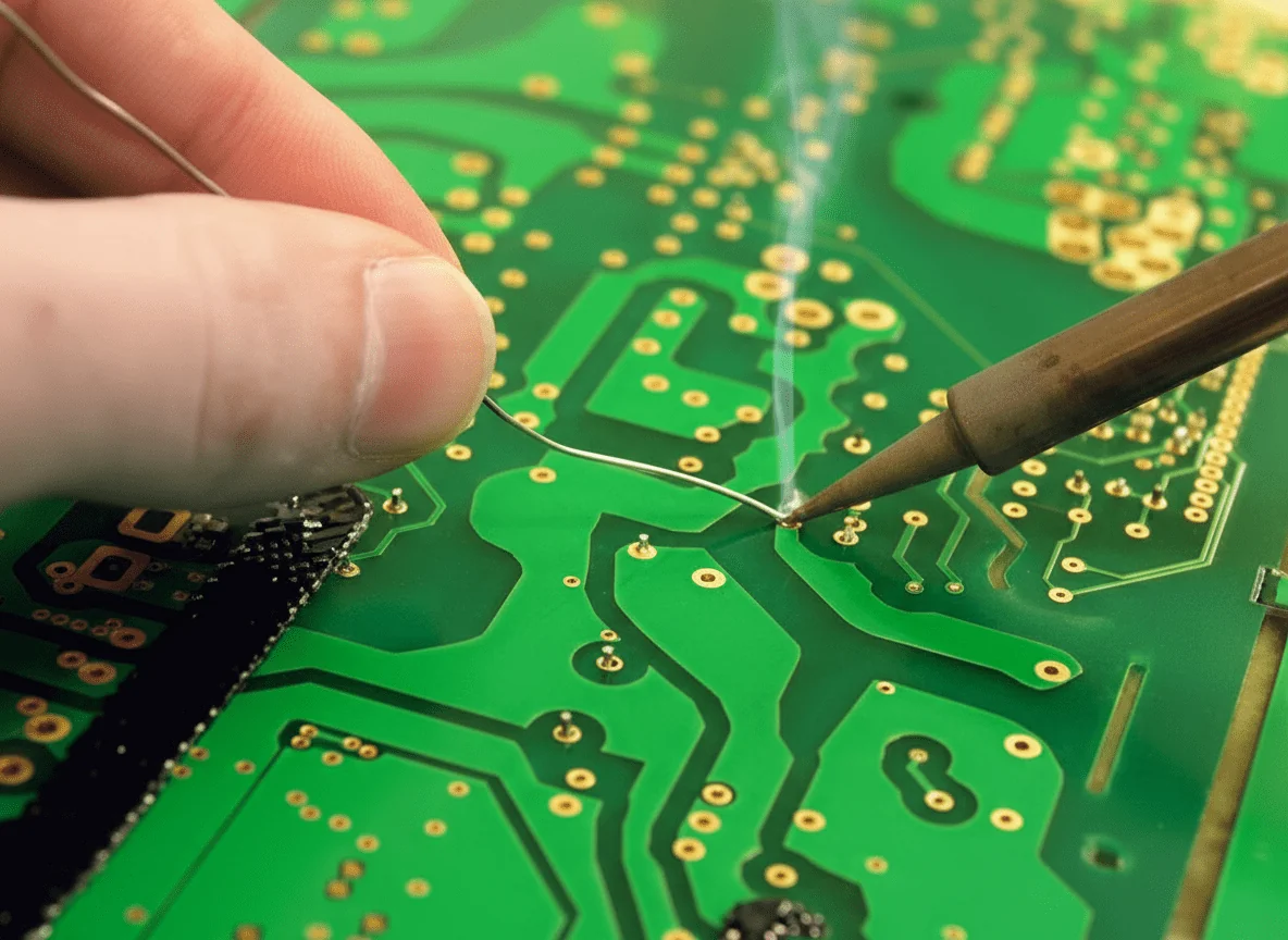
- Longer contact time: Lead-free wetting is measurably slower; iron tip dwell time must increase
- Higher iron temperature: 370-400°C for hand soldering lead-free versus 340-360°C for tin-lead
- Flux awareness: Lead-free fluxes activate differently at higher temperatures; operators need to understand when supplemental flux is appropriate
IPC-7711/7721 (Rework of Electronic Assemblies) and IPC-A-610 both contain lead-free-specific requirements for rework and inspection. Your inspection team must be trained on the visual differences between acceptable lead-free joints and defects — the matte appearance of a properly formed SAC305 joint is normal, not a defect.
Step 4 — Update Your Quality Plan
Your incoming inspection and quality plan should include:
- X-ray inspection or cross-sectional analysis on BGA joints to verify internal wetting and void content — BGA joints are not inspectable from the surface
- Shear testing on QFN and LGA packages per IPC-A-610 Class 3 requirements for high-reliability applications
- Temperature cycling testing (typically -40°C to +125°C, 500-1000 cycles) for Class 2 and Class 3 assemblies
- Drop shock testing (JEDEC JESD22-B111) for consumer products where drop survival is a specified requirement
Why Lead-Free Solder Matters for Your PCB Project
If you are designing a new product for commercial sale, lead-free solder is not optional — it is the default. The RoHS framework applies in the EU, China, Japan, South Korea, and increasingly through OEM supply chain requirements even in markets without explicit legislation. If you source components from global distributors, the lead-free versions are now the standard catalog items; tin-lead versions are often special-order with extended lead times and price premiums.
The design implications are concrete:
Component selection: Only components with peak reflow ratings of 260°C or higher are reliably assembled with standard SAC305 lead-free profiles. When evaluating components, check the moisture sensitivity level (MSL) rating and the peak reflow temperature in addition to the electrical specifications. A component datasheet that does not specify a peak reflow temperature should be treated as tin-lead-rated until confirmed otherwise.
Thermal management in design: Your PCB must tolerate 245-260°C peak temperatures during assembly. This constrains your laminate material choice — standard FR-4 (IPC-41026, Tg 135°C) tolerates those temperatures with a properly controlled profile, but profile overshoot or repeated reflow passes risk delamination. For boards that will see multiple reflow passes, consider FR-4 Tg 150°C or polyimide.
Solder mask and surface finish compatibility: Lead-free processing temperatures are compatible with ENIG (electroless nickel immersion gold), HASL (with appropriate thermal exposure limits), and OSP surface finishes. Verify that your specific finish combination is rated for your target peak temperature — some OSP formulations degrade above 250°C, and the ENIG process nickel thickness affects gold dissolution behavior at higher reflow peaks.
Frequently Asked Questions
What is lead-free solder made of?
The most common lead-free solder alloy is SAC305: 96.5% tin, 3% silver, and 0.5% copper. Tin is the base metal because it provides the best wetting characteristics and the most reliable metallurgical bond with copper and nickel component termination surfaces. Silver increases mechanical strength and lowers the melting point slightly compared to tin-copper alone. Copper restricts dissolution of board copper pads into the solder during reflow, preventing pad erosion. Other lead-free alloys include Sn99.3Cu0.7 (for wave soldering), Sn-Ag-Bi variants (for improved drop resistance), and Sn42Bi58 (for low-temperature assembly of heat-sensitive components).
What temperature does lead-free solder melt at?
SAC305 — the global commercial standard lead-free alloy — melts at 217°C (solidus) to 220°C (liquidus). For reliable wetting and joint formation during reflow soldering, the peak temperature must reach 245-260°C. This is approximately 34°C higher than the tin-lead eutectic (63/37), which melts at 183°C and reflows at 225-235°C. All components on a lead-free assembly must be rated for a peak reflow temperature of at least 260°C to survive the assembly process without damage.
Is lead-free solder weaker than leaded solder?
Lead-free solder is not uniformly weaker — it has different mechanical properties in different loading conditions. In thermal cycling fatigue (repeated temperature excursions from -40°C to +125°C), SAC305 performs equal to or slightly better than tin-lead, with slower crack propagation at the solder joint interface. In drop shock resistance, lead-free is genuinely weaker — it is harder and less ductile at room temperature, so it fractures rather than plastically deforming under impact. For applications where drop survival is a specified requirement — smartphones, wearables, portable medical devices — this is a real design constraint. For industrial control systems, automotive electronics, and telecom infrastructure where thermal cycling is the dominant failure mechanism, lead-free performs well.
Why does tin whisker risk increase with lead-free solder?
Lead acts as a tin whisker growth suppressant in the tin-lead microstructure. When lead is removed from the alloy, whisker growth becomes possible because the grain boundary conditions that allowed spontaneous tin crystallization are no longer inhibited by lead atoms. Mitigation strategies include alloying with small amounts of bismuth, antimony, or nickel to modify the grain structure; reflowing matte tin finishes to convert the surface to a more stable alloyed state; and applying conformal coating on high-reliability assemblies where whisker-induced short circuits would be unacceptable. IPC standards address whisker mitigation requirements for aerospace and defense applications, which have the most stringent documented whisker control programs.
How do I transition from tin-lead to lead-free assembly?
Transition requires process recipe changes, not just material substitution. Key steps: verify all components are rated for 260°C peak reflow temperature and identify alternatives for any that are not; develop a new reflow profile with higher peak (245-260°C), longer time above liquidus (30-60 seconds), and a controlled soak zone (60-90 seconds at 180-200°C); retrain assembly operators on the slower wetting kinetics and higher iron temperatures (370-400°C for hand soldering); update your quality plan to include X-ray inspection of BGA joints and drop shock testing where applicable; and update your IPC-A-610 inspection criteria to reflect the visual differences between acceptable lead-free joints and defects.
Does RoHS apply to my product?
RoHS 2 (Directive 2011/65/EU, as amended by RoHS 3 in Delegated Directive (EU) 2015/863) applies to all electrical and electronic equipment placed on the market in the EU. If you sell a product in Europe, it must be RoHS compliant. Similar requirements exist in China (China RoHS), Japan (JIS C 0950), and South Korea. Major OEMs impose RoHS requirements on their supply chains as a contractual condition even in markets without explicit legislation. Significant exemptions exist for military and aerospace (Category 8), certain medical devices (Category 8), and some industrial monitoring instruments (Category 9) — but the exemptions are narrowing under successive RoHS recasts, and the administrative burden of claiming an exemption is substantial.
Related Guides
- How to Solder Wires: The complete process for hand soldering wire connections, including temperature settings for lead-free solder and how to avoid the cold joint mistakes that plague beginners transitioning from tin-lead technique.
- What Is Conformal Coating?: How thin polymer coatings protect lead-free solder joints and PCB assemblies from moisture, vibration, and environmental damage — relevant for high-reliability applications where whisker mitigation and joint protection intersect.
- PCB Design Guidelines: The manufacturing engineer’s guide to designing boards that are compatible with lead-free reflow profiles, including laminate selection, surface finish trade-offs, and DFM principles for high-temperature assembly.
- Electronics Manufacturing Process Overview: How lead-free assembly fits into the broader EMS process — from design review through SMT assembly, testing, and box-build delivery.
- IPC-A-610 Acceptance Standards: The workmanship standards that define acceptable and defective solder joints for lead-free assemblies across IPC Classes 1, 2, and 3.
Published for WellCircuits — Professional PCB Manufacturing and Assembly