Impedance-Controlled PCB Boards: Ensuring Signal Integrity
Introduction
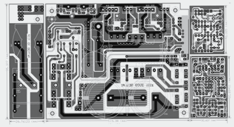
An impedance-controlled PCB (Printed Circuit Board) is designed to manage signal trace impedance, crucial for high-speed and high-frequency applications. Impedance control regulates signal resistance to prevent distortion, ensuring proper signal transmission without degradation.
Key Considerations in PCB Design
- Material Selection: Materials with low resistivity are essential for maintaining desired impedance levels and high-quality performance.
- Challenges with Tin Plating: Issues like discoloration and oxidation during tin plating can lead to high impedance and poor electrical conductivity.
- Frequency Impact: Changes in impedance due to factors like etching and trace width must be controlled to minimize signal distortion.
- Component Placement: Careful component placement is crucial for optimal signal quality and performance.
- False Copper Exposure: Uneven ink application during the curing process can expose copper traces, leading to potential short circuits.
Reasons for False Copper Exposure
False copper exposure in PCB manufacturing occurs due to uneven ink application during the curing process. This issue can result in incomplete protection of copper traces, potentially causing short circuits. Detecting and addressing this problem is vital to maintain the integrity and reliability of the PCB.
Common Issues in PCB Manufacturing: False Copper Exposure
-
Improper Solder Mask Process:
During solder mask application, using the wrong hole plugging method can result in incomplete filling and copper exposure. To avoid this, ensure proper hole plugging procedures and quality control.
-
Ink Residue in Heavy-Duty Board Holes:
If ink residue is left in holes, it can hinder proper hole filling during printing, leading to false copper exposure. Thoroughly clean the holes before reapplying the solder mask.
-
Improper Hole Plugging Due to Flat Printing Table:
Placing boards on a flat printing table can obstruct air flow, causing incomplete hole plugging and false copper exposure. Adjust the printing setup for better air circulation.
-
Lack of Personnel Inspection:
Inadequate personnel inspection can result in missed issues like false copper exposure. Enforce regular and thorough checks during production to prevent defective boards from progressing.
Recommendations to Address False Copper Exposure
When false copper exposure is identified, it’s crucial not to use the board to prevent damage to components. Defective boards should be returned to the factory for rework or remanufacturing. Implementing stringent quality control measures and enhancing staff training can effectively reduce false copper exposure occurrences.