Advanced PCB Via Solutions: Tenting, Filling & Plugging Techniques for High-Density Electronics
Why Modern PCB Manufacturing Demands Advanced Via Solutions
As hardware complexity increases exponentially, traditional PCB manufacturing techniques struggle to meet today’s demands. International electronics manufacturers face critical challenges:
- Current transfer between multiple PCB layers
- Signal exchange across different board layers
- Reliable soldering with ultra-high component density
These challenges require specialized via processing techniques to ensure proper board fabrication. Three advanced solutions have become industry standards for high-density PCB manufacturing:
- Via Tenting
- Via Filling
- Via Plugging
Understanding PCB Vias: The Foundation of Multi-Layer Design
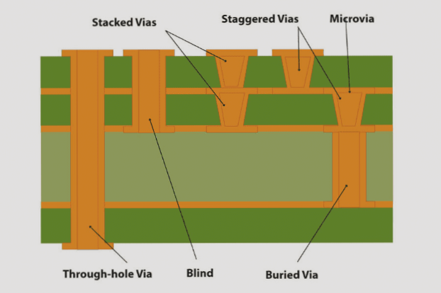
A via is essentially a conductive tunnel connecting traces across different PCB layers. This ingenious solution enables:
- Significant hardware size reduction
- Improved functionality in compact designs
- Efficient multi-layer connectivity
Modern PCB via technology allows designers to work with multiple layers as if they were one continuous surface, dramatically shrinking board footprint while maintaining performance.
Via Tenting: Protection Against Solder and Corrosion
What is Via Tenting and When is it Needed?
Via tenting addresses critical manufacturing challenges in high-density PCB assembly:
- Preventing solder bridging in BGA (Ball Grid Array) applications
- Avoiding unwanted solder filling during wave soldering
- Protecting exposed copper from oxidation and corrosion
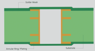
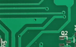
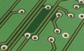
The process involves covering both the annular ring and via hole with solder mask, creating an isolation barrier. This is particularly crucial for:
- Components with minimal clearance
- Applications using via-in-pad technology
- Environments prone to corrosion
Via Filling: Complete Hole Occlusion for Maximum Protection


Filled and Covered Vias
This PCB via filling technique uses Liquid Photo Imageable (LPI) solder mask to completely fill via holes. Key characteristics:
- Non-conductive epoxy or resin filling
- Solder resist ink coverage (one or both sides)
- High process reliability for critical applications
Filled and Capped Vias for BGA Applications
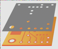

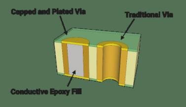
This advanced solution combines the benefits of via filling with preserved pad plating, making it ideal for:
- BGA component mounting
- Via-in-pad implementations
- Applications requiring enhanced current conductivity (when using conductive fill)
“Filled and capped vias represent the gold standard for high-reliability PCB manufacturing, particularly in complex BGA layouts.”
Via Plugging: Partial Filling for Specific Applications



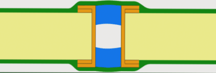
Key Differences from Via Filling
Via plugging involves partial filling of the via hole, creating a “closed” rather than completely filled structure. This technique offers:
- Material cost savings versus complete filling
- Flexibility in coverage options
- Effective solder prevention
Plugged Via Variants
1. Basic Plugged Vias:
- Partially filled with non-conductive material
- No solder mask coverage
2. Plugged and Covered Vias:
- Partial filling combined with LPI coverage
- Enhanced protection for demanding applications
Choosing the Right Via Solution for Your PCB Project
When selecting between via tenting, filling, or plugging, consider these factors:
- Component density and spacing requirements
- Soldering process (wave, reflow, etc.)
- Environmental exposure conditions
- Current carrying requirements
- Budget and manufacturing constraints
For international buyers sourcing PCB manufacturing in China, understanding these advanced via techniques ensures you receive boards that meet your exact technical specifications while maintaining competitive pricing.
