The Essential Guide to Silk Screen Technology in PCB Manufacturing
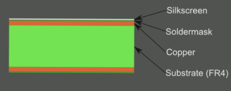
Silk screening, a critical process in printed circuit board (PCB) production, involves applying non-conductive epoxy ink markings to identify components, test points, logos, and other essential elements. This cost-effective labeling solution enhances assembly accuracy and troubleshooting efficiency for both manufacturers and engineers.
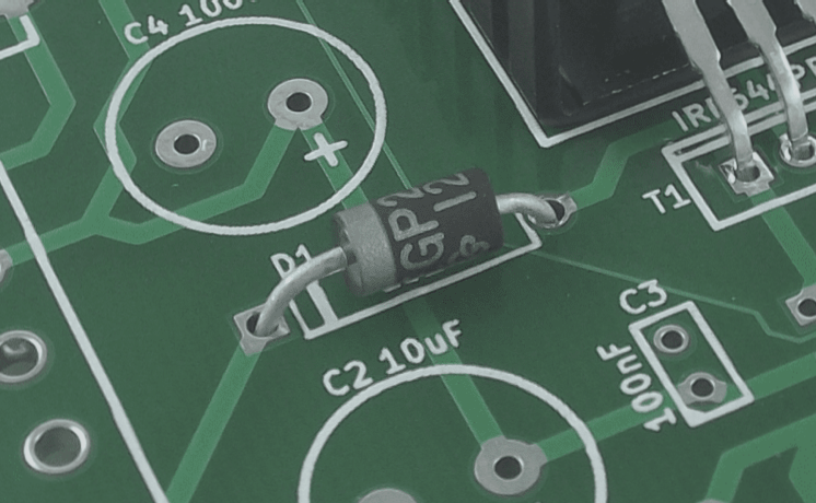
Understanding PCB Silk Screen Fundamentals
Modern PCB silk screening utilizes specialized epoxy inks available in standard colors:
- Black – Most common for high contrast visibility
- White – Preferred for dark substrate boards
- Yellow – Used for specific visibility requirements
The ink formulation ensures durability throughout the PCB’s lifecycle while maintaining excellent electrical insulation properties. Most PCB design software includes standard font libraries, though custom typography can be implemented when required.
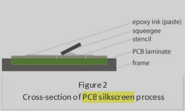
Three Primary Silk Screen Application Methods
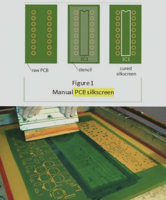
1. Manual Screen-Printing: Traditional Approach
Best suited for designs with:
- Line widths exceeding 7 mil (0.007″)
- Registration tolerance of 5 mil
This cost-effective solution uses nylon stencils to transfer ink onto the laminate, followed by oven curing. While offering simple setup, it provides the lowest precision among application methods – ideal for prototype PCB manufacturing or boards with generous tolerances.
2. Liquid Photo Imaging (LPI): Enhanced Precision
Recommended for applications requiring:
- Line widths down to 4 mil
- Higher positional accuracy
LPI mirrors the solder mask application process, using UV-exposed photoimageable epoxy that delivers superior resolution compared to manual methods. This makes it the preferred choice for high-density interconnect (HDI) PCBs and complex circuit designs.
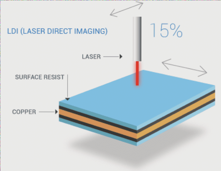
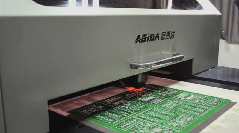
3. Direct Legend Printing (DLP): Maximum Accuracy
The most advanced solution featuring:
- CAD-driven inkjet application
- Instant UV curing
- Exceptional precision for fine details
While offering the highest quality results, DLP carries a premium cost and has limitations with silver-finished boards. This method is particularly valuable for high-reliability PCB assemblies where marking clarity is critical.
Strategic Benefits of Proper Silk Screen Implementation
Effective silk screen application delivers measurable advantages:
- Error reduction during assembly and maintenance
- Time savings in component identification
- Improved traceability throughout product lifecycle
For international buyers sourcing from PCB manufacturers in China, understanding these benefits helps optimize both quality and cost-efficiency in their supply chain.
Best Practices for Silk Screen Design
To maximize the value of your PCB silk screening:
- Maintain minimum 0.25mm clearance between component outlines and pins
- Ensure line widths ≥6 mil for readability
- Avoid printing over solderable surfaces
- Consider single-side application for cost-sensitive projects
“Proper silk screen implementation can reduce assembly errors by up to 30% while significantly decreasing troubleshooting time – a critical factor for high-volume PCB production.”
Cost Optimization Strategies
International buyers can achieve significant savings by:
- Specifying standard ink colors
- Limiting silk screen to essential surfaces
- Choosing the appropriate application method for their precision requirements
These considerations are particularly important when working with global PCB suppliers to balance quality and budget requirements.

Partnering with Reliable PCB Manufacturers
When selecting a PCB fabrication partner in China, verify their:
- Silk screen application capabilities
- Quality control processes
- Experience with international export standards
WellCircuits combines advanced silk screen technologies with export-grade manufacturing standards, making them a preferred choice for global electronics companies seeking high-quality PCB solutions.
