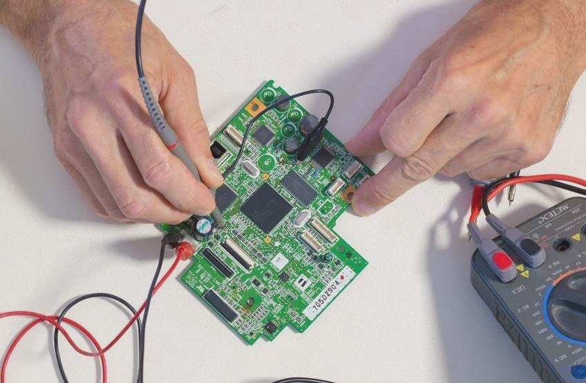
How to Design a Printed Circuit Board Yourself: A Comprehensive Guide

Understanding PCB Basics for DIY Design
Printed circuit boards (PCBs) form the backbone of modern electronics, found in everything from smartphones to industrial machinery. As a leading PCB manufacturer in China, WellCircuits Electronics Services provides this step-by-step guide to help international buyers understand how to design a PCB from scratch for prototyping or small-scale production.
Essential Components of PCB Design
- Substrate Material: Typically FR-4 fiberglass for rigidity and insulation
- Copper Layer: Conductive pathways etched onto the substrate
- Solder Mask: Protective green/brown coating preventing short circuits
- Silkscreen: Component labels for assembly guidance
Step-by-Step PCB Design Process
1. Substrate Preparation and Copper Lamination
The foundation begins with a non-conductive substrate laminated with copper foil. For high-quality PCB fabrication, we recommend using 1oz copper for standard applications.
2. Circuit Pattern Transfer
Using photolithography, your design transfers to the copper layer:
- Apply UV-sensitive photoresist
- Expose through your circuit pattern mask
- Develop to remove unexposed areas
3. Etching and Drilling
Chemical etching removes unwanted copper, leaving only your circuit traces. For multi-layer PCB assembly, precision drilling connects internal layers via plated through-holes.
“Proper hole plating ensures reliable interlayer connections – a critical factor in professional PCB manufacturing.” – WellCircuits Engineering Team
4. Solder Mask Application
The iconic green coating serves multiple purposes:
- Prevents solder bridges between components
- Protects copper from oxidation
- Provides electrical insulation
5. Silkscreen Marking
Component labels and logos applied via epoxy ink help with:
- Accurate part placement during PCB assembly services
- Troubleshooting and repairs
- Quality control verification
Critical Testing Procedures
Before deploying your DIY PCB, conduct these essential tests:
Electrical Testing
- Continuity checks for open circuits
- Insulation resistance measurements
- High-voltage dielectric tests
Automated Optical Inspection (AOI)
Fast, accurate detection of:
- Trace defects
- Solder mask imperfections
- Silkscreen errors
When to Partner with a Professional PCB Manufacturer
While DIY PCB design works for prototypes, consider China PCB manufacturing services for:
- High-volume production runs
- Complex multi-layer designs
- Specialized materials (high-frequency, flexible PCBs)
- Strict quality compliance (IPC Class 2/3)
Why Choose WellCircuits for Your PCB Needs?
As a trusted PCB supplier for international trade, we offer:
- DFM (Design for Manufacturing) analysis
- Fast-turn prototyping (24-48 hours)
- Competitive MOQs for export businesses
- Complete documentation for customs clearance
For more guidance on how to select the right PCB materials or best PCB manufacturing processes, visit WellCircuits Electronics Services – your partner in global electronics trade solutions.
