PCB Layers Overview
-
Mechanical Layer
The mechanical layer defines the structure and appearance of the PCB circuit board, including external dimensions, data markers, and assembly instructions.
-
Forbidden Wiring Layer
The forbidden wiring layer sets boundaries for copper layout, ensuring electrical traces stay within designated areas.
-
Silkscreen Layers
The top and bottom overlay layers display component designators and characters on the PCB.
-
Pad Layers
The top paste and bottom paste layers indicate exposed copper pads on the PCB, essential for soldering components.
-
Solder Layers
The top solder and bottom solder layers are covered with solder mask, appearing silvery white due to their negative output.
-
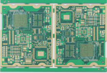
Multilayer
The multilayer encompasses all PCB layers, providing a comprehensive view of the circuit board.
-
Signal Layer
The signal layer organizes wiring on the board, offering multiple signal layers for complex designs.
-
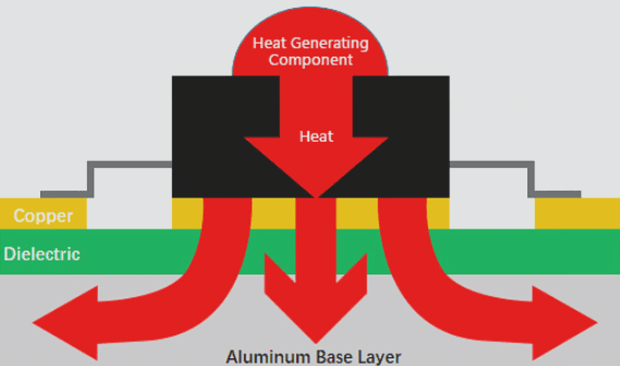
Internal Plane Layer
Internal power and ground planes aid in organizing power and ground connections for multilayer boards.
-
Solder Mask Layer
The solder mask layer protects areas from solder except for pads, crucial for soldering components accurately.
-
Paste Mask Layer
The paste mask layer aids in machine soldering of surface-mounted components, ensuring proper application of solder paste.
-
Keep Out Layer
The keep out layer defines areas where components and wiring are permitted on the PCB, restricting automatic layout and routing beyond specified zones.
-
Silkscreen Layer
The silkscreen layer is used for printed information and annotations, providing clarity on component placement and other details.

Pads and Vias on PCBs: A Guide to Multilayer Systems
When designing a PCB, it is crucial to ensure that pads and vias are strategically placed to establish electrical connections across different conductive pattern layers. This is where the concept of multilayer PCBs comes into play.
Understanding Multilayer PCBs
Multilayer PCBs consist of specialized layers that allow pads and vias to traverse the entire board, facilitating seamless electrical connections. Without these layers, pads and vias may not be visible, impacting the functionality of the PCB.
The Role of the Drill Layer
In PCB manufacturing, the drill layer is essential for providing drilling information. This information includes detailing which pads and vias require drilling to ensure proper connectivity. Protel 99 SE offers two primary drilling layers: Drillgrid, which serves as a drilling indication map, and Drill Drawing, which provides a drilling diagram.
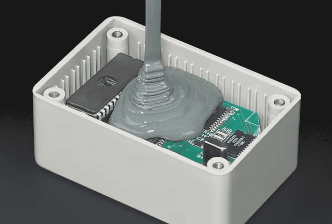
Looking for PCB Manufacturing Services?
If you have any PCB manufacturing needs or require further assistance, feel free to contact me. Our team is here to help you with all your PCB requirements.