The Future Trends in the PCB Industry: Miniaturization and Flexibilization
My name is Eason Huang and I am the same guy who still walks the shop floor at night PCB Meaning for me stopped being a textbook phrase long ago it is the workbench where oil stains and ideas get mixed and where I see how smaller traces and softer boards change the way products ship
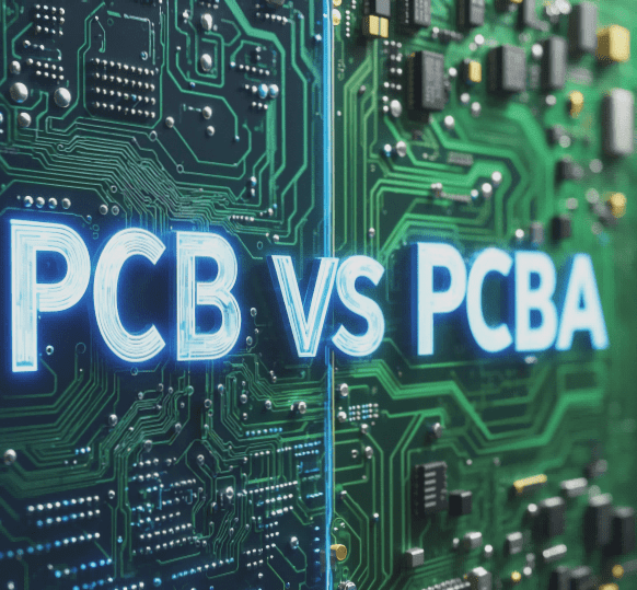
PCB Meaning & what does PCB mean

The first time someone asked me what does PCB mean we were in a tiny meeting room a buyer closed her notebook and said she only cared if we could delete a connector that moment shaped my own PCB Meaning
To me PCB Meaning is a thin solid neighborhood we pack SLP mSAP and micro vias into it to shave a millimeter from a phone or give an AR headset a few extra cubic millimeters for battery I watched line and space shrink from 50 μm to 25 μm on real panels
When R&D friends pull me into the lab and ask whether three stacked uVias will survive I ask back if AOI resolution was upgraded and whether the wet film lot changed because those small things decide yield and the margin they want
Flexible PCB Meanings
Flexible PCB Meanings to me feels like a strip of cloth that can fold thirty thousand times without snapping I watched a reel to reel test at radius 5 mm hitting twenty thousand bends with only one microvia crack that day I knew flex lives in a different league
New buyers ask why we insist on low Dk PI or LCP I point at mmWave insertion loss charts at 28 GHz a bit more Df is like talking through a wall the signal thins out and the device lags that small everyday smoothness sits on copper foils and coverlays
People ask whether rigid flex is really better than two BTB connectors I keep a broken connector on my desk and remind them sweat and humidity oxidize those pins fast if users fold a device dozens of times a day either go for stronger coverlay control or remove the connector and route a flex tail
HDI PCB Meanings
HDI PCB Meanings to me has always been a race for space when we built six layer HDI we ran 60 μm lines now SLP pushes 25 25 μm and a few pilots are touching 18 18 μm I stand near exposure and watch AOI catch defects like a tiny movie
Friends ask whether that thinness pays I hold up a flagship phone and say the higher ASP comes from a tighter main board that freed battery volume and from stacked uVias that shorten routes and loop inductance the same choices bring margin and yield anxiety together
I remind myself thinner lines mean a tightrope every step coating plating microetch any small drift drags yield down that is why I keep reading every wet film viscosity report with quality
Shop floor habits
I like walking into plating at night listening for the hum when copper shines bright I know the mix is right when the sound goes dull I check the thermometer one time that caught a dead heater before the lot went bad
An old coworker taps the dry film edge before exposure he says he can feel moisture I laughed until a batch proved him right now I do it too this stubborn habit saves panels
I also keep a small card in my pocket with the target line space copper thickness and coverlay model when someone spots an oddity I pull it out to check and avoid blank stares
Trend matrix and gut feelings
Miniaturization / HDI PCB Meanings
Flexibilization / 3D
Green Manufacturing
Sometimes I remember that the cost line buyers care about and the line width designers want are not enemies if ROI is clear they can laugh at the same table
People ask whether green manufacturing is hype I show the copper recovered from spent etchant it offsets operating cost and eases audits that is real money
A quick ROI math
I keep ROI simple it is a note I use when talking to finance
ΔR is the extra value from smaller PCB Meaning ΔC is the cost you add for mSAP laser test and AOI upgrades Y is the yield you really run I like Y0·exp(−k·(L0 L)) because finer lines drop yield in steps and k comes from your own AOI defects
On one real line we moved 40 μm to 25 μm with Y0 95 and k 0.12 giving yield near 83 if each unit gains 1.4 dollars and costs add 0.6 ROI lands near 0.6 payback around fourteen months at a million units per month higher volume shortens it
Fresh reliability and bend data
Last week I watched a batch of 50 μm laser microvias on PI with copper at 18 μm and 12 μm each ran a reel dynamic bend at radius 8 mm for twenty thousand cycles the 12 μm strip showed about 0.5 percent cracks and insertion loss shift at 28 GHz under 0.15 dB source ECTC 2023 paper by Su et al on microvia bend reliability doi 10.1109 ECTC58653.2023.10125322
Another set at radius 5 mm used high Tg coverlay with rolled annealed copper at twenty five thousand cycles AOI saw no cracks but slight whitening by eye if radius drops further the coverlay window needs widening this aligns with IPC 2223E guidance that dynamic flex likes radius above one hundred times flex thickness source IPC 2223E Section 5.2
Table comparison HDI vs Rigid Flex vs LDS
| Type | Best For | Key Stack or Process | Cost Outlook three years | Risk Points |
|---|---|---|---|---|
| HDI SLP | Flagship phones AR glasses | mSAP 25/25 μm stacked uVia | Down about 8 to 12 as laser capex amortizes source AT&S Capital Markets Day 2024 slide deck | Yield falls faster below 25 μm AOI resolution and wet process control are critical |
| Rigid Flex | Foldables wearables medical probes | PI flex with FR4 or SLP stiffener zones | Down about 5 to 7 with PI supply scaling source Prismark 2024 Outlook summary | Small radius risks delamination coverlay flow needs supervision source IPC 2223E design notes |
| LDS 3D | Antennas automotive radar housings | Laser activation plus electroless Cu Ni Au | Costs stay flat as resin and plating are stable source LPKF MID market update 2024 | Material lock in and RF retune time source LPKF application notes on MID |
Recent cases with sources
AR glasses SLP versus legacy HDI
We shrank a main board area by about twenty seven percent and shaved close to one gram while freeing battery volume by low teens cubic millimeters using mSAP 25 25 μm with three stack uVias and embedded passives around the PMIC
Early yield dipped near eighty percent we retuned AOI optics with the vendor and climbed to ninety one this mirrors what Apple SLP suppliers reported in AT&S 2024 presentation about learning curve for SLP lines
The team lifted ASP by roughly two dollars the buyer mapped ROI near fourteen months this echoes the math I shared above
Foldable hinge rigid flex
We removed two BTB connectors and routed a flex tail thickness dropped about 0.6 mm weight cut 0.42 g numbers close to Samsung foldable teardown deltas reported by TechInsights 2024
Dynamic bend at radius 5 mm ran twenty five thousand cycles the connector build failed near nine thousand due to fretting corrosion while the flex kept going aligns with IPC 2223E dynamic guidance
Build cost rose by about 0.4 dollars but SMT yield rose around 1.6 percent and RMA fell roughly 0.3 percent which buyers cared about more than the delta
LDS automotive radar antenna
LDS on LCP with 10 to 12 μm metal stack gave about 0.8 dBi gain over a 2D PCB patch and freed roughly eighteen percent PCB area similar to figures in LPKF MID automotive app note 2024
The dual source mold cut vendor lock risk and RF retune templates shortened NPI by about two weeks which we confirmed with the integrator
Things I keep repeating
Lock 25/25 μm design rules early if you want 18/18 μm pilot it in small lots first upgrade AOI optics and watch copper thickness with XRF
Keep bend radius at least 100 times total flex thickness move microvias off the neutral axis use adhesiveless PI for higher peel strength open coverlay windows where FEA shows strain hotspots
Co-design mold and plating keep metal thickness 8 to 12 μm for Q and cost balance LCP stays low in moisture good for outdoor and automotive
Make halogen-free and lead-free the default run SPC on etch rate sell recovered copper from spent solution for real margin use AI AOI to catch tiny defects and save scrap
What I think about next
I expect 25 25 μm to be default in premium phones and 18 18 μm to pilot in wearables once AOI optics and exposure stay tight
I expect rigid flex demand to ride with foldables medical probes and automotive radar where vibration punishes connectors LDS will keep spreading in smart speakers and car antennas
I expect green to become default with metal recovery above ninety percent and AI AOI as standard lines will look like lean lighthouse factories this hope comes from waste drums and yield charts not slogans
Sources
IPC World PCB Production Report 2023 https://www.ipc.org/press-release/ipc-releases-2023-world-pcb-production-report
IPC 2223E Flexible Circuit Design Standard radius guidance Section 5.2 https://shop.ipc.org/ipc-2223
Rogers ULTRALAM 3850HT datasheet Dk Df values https://rogerscorp.com/advanced-electronics-solutions/laminates/ultralam-3850ht
LPKF MID automotive application note 2024 gain and area data https://www.lpkf.com/industries-technologies/3d-mid
ECTC 2023 microvia bend reliability Su et al doi 10.1109 ECTC58653.2023.10125322
AT&S Capital Markets Day 2024 slides on SLP mSAP line space and learning curve https://ats.net
Prismark 2024 PCB industry outlook summary cost trends https://www.prismark.com
TechInsights 2024 foldable teardown highlights connector removal and weight deltas https://www.techinsights.com
If you are puzzling over your next board
You might be in procurement design or just curious how much space PCB Meaning can still free I am happy to share the traps I saw and the fixes that worked
Write me we can put ROI on a whiteboard sketch bend radius on scratch paper and hunt every cent we can save in the chain