Differences in High-Density Interconnect (HDI) PCBs
High-Density Interconnect (HDI) printed circuit boards (PCBs) have transformed electronic technology. Known by various names like Sequence Build (SBU) and Microvia Process (MVP), the term “HDI” was standardized by the IPC (Institute for Printed Circuits) for global use in the PCB industry.
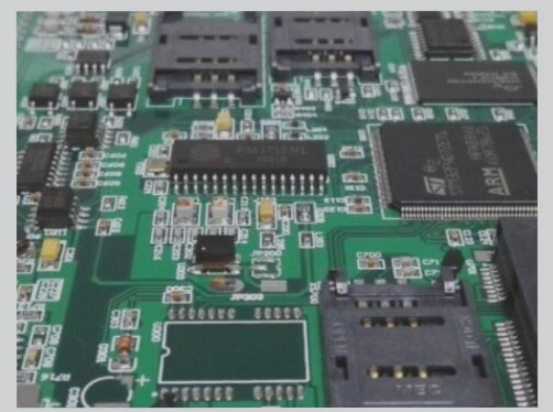
HDI PCBs are recognized for their high-density interconnections, enabling the use of smaller components and the creation of more powerful devices. This technology is essential for modern electronics like smartphones, tablets, and wearable tech, maintaining high performance while reducing device size.
Advantages of HDI PCBs
- Size: HDI boards accommodate more connections in a smaller area, achieving higher density with fewer layers, leading to more efficient circuits.
- Design Flexibility: Greater capacity allows for complex circuitry, reducing the need for multiple boards and enabling faster signal processing.
- Reliability: Small blind vias improve electrical performance and reliability, surpassing traditional boards in reliability.
- Complex Packages: HDI handles densely packed components that are challenging to mount on traditional boards.
- Smaller, Lighter Boards: Enables smaller, lighter boards with more features, ideal for compact devices.
- Functionality: Integrates multiple traditional PCBs into a single board, simplifying design and enhancing system reliability.
- Signal Integrity: Enhances electrical performance critical for high-speed applications.
HDI Board Design Challenges
- Miniaturization: Involves microvias requiring precise drilling and specialized fabrication expertise.
- Layer Stacking: Incremental layer addition demands careful planning to optimize signal routing.
- Thermal Management: Effective solutions like heat sinks are crucial due to increased heat generation.
- Impedance Control: Critical for high-speed signals, requiring careful routing for signal integrity.
In conclusion, HDI PCBs are crucial for modern electronic devices, offering compact size, enhanced functionality, and superior reliability. Specialized knowledge and attention to detail are essential for designing these boards to overcome their unique challenges.
Material Selection and Design Considerations in HDI PCB Design
The Importance of Material Selection in HDI PCB Design
In PCB design, material and component selection are crucial, especially for High-Density Interconnect (HDI) PCBs. The choice of materials not only affects electrical performance but also impacts the overall cost of the final product. Selecting the right materials is essential to balance performance, durability, and cost-effectiveness in HDI applications.
Advantages of Micro-Via Stacking
HDI technology allows for stacking micro-vias, a method that can save space, minimize signal delay, and reduce interference. By leveraging micro-via stacking, designers can create more compact layouts and enhance the functionality of PCBs, particularly in high-performance devices like smartphones.
Every Layer Interconnect (ELIC) Technology
Every Layer Interconnect (ELIC) technology, popular in smartphone circuits, offers benefits such as smaller spacing, the elimination of mechanical holes, and reduced board area usage. However, asymmetrical stacking designs may cause warping during manufacturing, emphasizing the importance of a well-planned stack-up design.
Component Placement and Density
HDI technology requires high-density component placement, necessitating careful consideration to ensure soldering, installation, and maintenance feasibility. Maintaining uniform track widths and minimizing line spacing is crucial to prevent circuit malfunctions in HDI designs.
Cost and Quality in HDI Design
Cost and quality are primary concerns in HDI design due to intricate manufacturing processes and expensive materials. Balancing cost-effective solutions with high-quality standards is essential to meet consumer expectations while ensuring profitability.
Key Considerations Before Implementing HDI
- Skill Combination: Specialized skills are required for HDI PCB design, emphasizing the need for careful planning to avoid costly design changes post-manufacturing.
- Planning: Detailed design phases are crucial to prevent errors that could disrupt manufacturing timelines and budgets.
Integrating Design for Manufacturing (DFM)
Integrating Design for Manufacturing (DFM) principles into HDI PCB design is essential to ensure feasibility for production and minimize fabrication errors. Collaboration with manufacturers and utilizing DFM tools can enhance design outcomes and reduce risks.
In conclusion, successful HDI PCB design involves meticulous material selection, via technologies, component placement, and design planning. Balancing complexity with manufacturing constraints and cost considerations is key to producing functional, cost-efficient HDI PCBs. Collaboration with experienced manufacturers and adherence to DFM principles can lead to successful production outcomes.
If you have any questions about PCB or PCBA, feel free to contact me at info@wellcircuits.com.