PCB Proofing and Welding Process: A Comprehensive Guide
Introduction to PCB Proofing
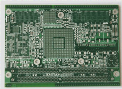
PCB proofing, short for Printed Circuit Board proofing, is a critical phase in the development of electronic systems. A PCB serves as the foundation for electronic components, providing essential electrical connections through a printed circuit manufacturing process.
Understanding PCB Proofing
PCB proofing involves the trial production of printed circuit boards before mass manufacturing. This phase allows for testing the PCB design and functionality on a small scale, ensuring optimal performance before full-scale production. It is a crucial step in verifying the circuit’s performance and design integrity.
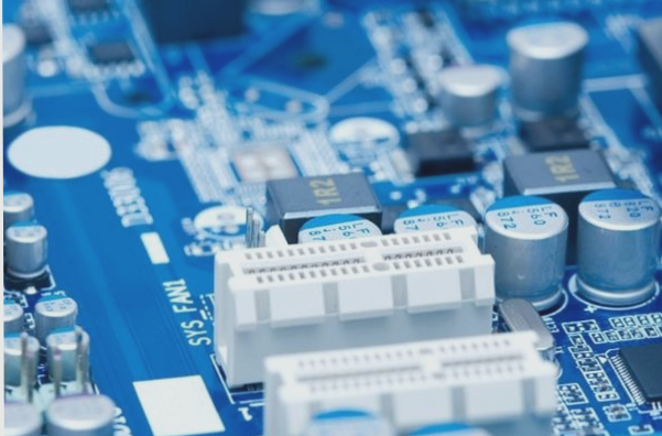
PCB Welding Process Overview
The PCB welding process is essential for assembling and ensuring the functionality of the PCB. It includes manual component insertion, soldering, inspection, and trimming to create reliable circuits.
Key Steps in PCB Welding Process:
- Component Categorization: Components are categorized according to the bill of materials (BOM).
- Insertion: Manual insertion of components into designated PCB locations.
- Soldering: Components are soldered using techniques like wave soldering or hand soldering.
- Cutting Leads: Trimming excess leads to prevent short circuits.
- Inspection: Thorough inspection for defects like improper soldering or missing components.
- Trimming: Final trimming to prepare the PCB for use or further testing.
Component Processing Requirements in PCB Welding
Solderability Treatment
Before component insertion, verify solderability for reliable solder joints.
Pin Alignment and Pitch
Ensure proper alignment between component pin pitch and PCB land hole pitch for effective soldering.
Lead Shape and Heat Dissipation
Optimize component lead shape for efficient heat dissipation and mechanical strength post-soldering.
Component Insertion Process on PCB
Component Insertion Best Practices for PCB Assembly
- Follow a systematic insertion order for components on the PCB to ensure a smooth assembly process:
- Start with lowest-profile components and progress to higher ones.
- Insert smaller components before larger ones.
- Lighter components should be inserted before heavier ones.
- Easier-to-insert components should come before more challenging ones.
- General components should be inserted before specialized ones.
Component Orientation
After insertion, ensure that component markings, such as part numbers and polarity indicators, are oriented for easy readability. Align markings left-to-right for optimal viewing during inspection or troubleshooting.
Polarity Considerations
For components with polarity requirements, strictly adhere to the polarity markings on the PCB drawing to prevent circuit failure due to misinstallation.
Insertion Alignment and Aesthetics
Insert components with consistent spacing and alignment to maintain a neat and organized layout. Avoid angled, overlapping, or three-dimensional arrangements. Ensure component leads are of uniform length on both sides for a balanced and professional appearance.
Solder Joint Quality Requirements
- Ensure solder joints exhibit:
- Mechanical strength to withstand operational stresses and handling.
- Reliable electrical conductivity to prevent intermittent connections or failures.
- Smooth and clean surfaces free from contaminants for long-term reliability.
Electrostatic Protection in PCB Assembly
Electrostatic Protection Principles
- Prevent Static Electricity Build-Up:
- Implement measures to control static buildup and protect sensitive components.
- Rapid Static Discharge:
- Eliminate existing static charge through proper grounding and discharge protocols to prevent damage to electronic components.
Static Electricity Protection Methods
- Grounding and Discharge Channels:
- Ground all components prone to static electricity and establish independent grounding systems to minimize the risk of component damage.