The Evolution of Circuit Boards
- Circuit boards play a crucial role in optimizing electrical layouts and mass-producing fixed circuits.
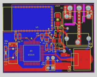
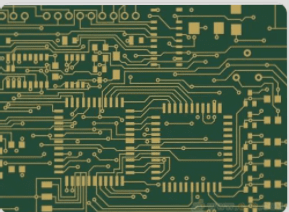
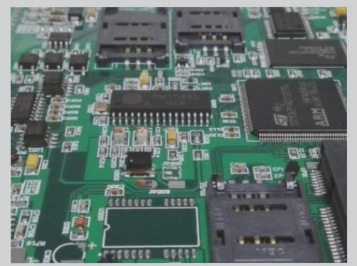
- They are known as PCBs (Printed Circuit Boards) and come in various types such as ceramic, aluminum, and high-frequency boards.
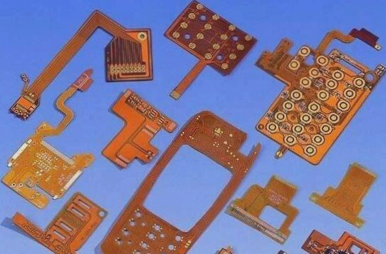
- Rigid-flex boards combine the features of flexible and rigid boards for innovative product designs.
- Single-sided, double-sided, and multilayer circuit boards cater to different complexity requirements.
Designing PCBs
- Start by preparing circuit schematics and creating a new PCB file.
- Plan the layout, include netlists and components, and automatically lay out the design.
- Adjust the layout, analyze network density, and set up wiring rules.
- Use EDA software like Altium Designer for multilayer PCB design following specific design rules.
For a successful PCB design, follow guidelines on trace and component placement, routing, and signal integrity. Different design rules may apply based on the circuit complexity, and software automation can significantly impact design quality.
Setting Up Multilayer PCBs
- Begin by creating a new PCB file for your project.
- Select File > New > PCB to start the design process.
- Altium Designer offers tools for managing layers and optimizing the PCB layout.

PCB Layer Configuration
Currently, the PCB design consists of two layers: TopLayer and BottomLayer. To enhance the design, users can modify settings on the right-hand side. By making adjustments, a four-layer PCB can be set up with GND and VCC layers. Importing the compiled schematic enables the creation of the layout for the four-layer board.
Operational Skills
The operational skills required for each layer of the PCB are similar to those for a single-sided board. Therefore, careful consideration is necessary during the design phase to ensure optimal functionality.
Creating a New PCB File
- If you have a project in mind, start by creating a new PCB file within your project.
- Go to File > New > PCB.
Layer Management
Upon creating a new PCB file, it initially contains only the TopLayer and BottomLayer. To access more layers, open the layer management interface for further customization.
At present, the visible layers are limited to TopLayer and BottomLayer. Users can adjust settings on the right-hand side to include additional layers such as GND and VCC in the four-layer PCB configuration. Importing the schematic design enables the creation of a comprehensive layout for the four-layer board.