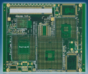
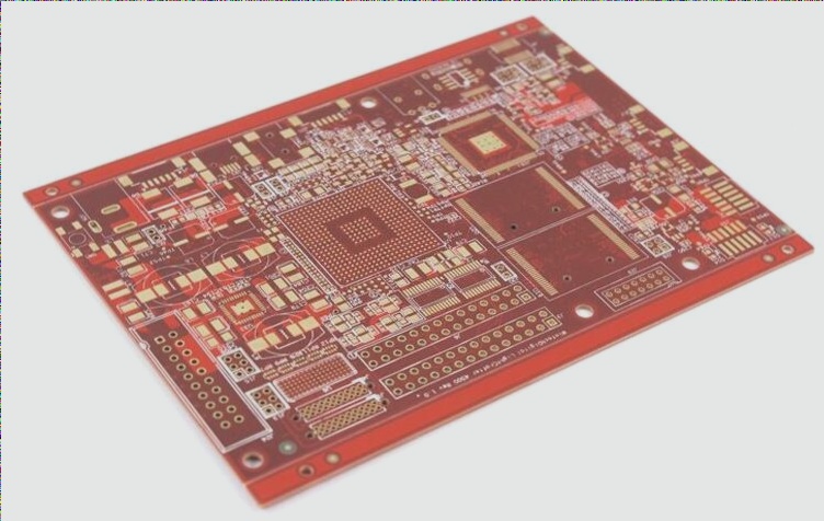
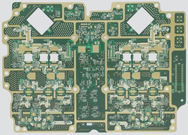
WellCircuits Limited Design Capabilities
- The highest signal design rate: 10Gbps CML differential signal
- The highest number of PCB design layers: 40 layers
- Minimum line width: 2.4mil
- Minimum line spacing: 2.4mil
- Minimum BGA PIN spacing: 0.4mm
- Minimum mechanical hole diameter: 6mil
- Minimum laser drilling diameter: 4mil
- Maximum PIN number: 63000+
- Maximum number of components: 3600
- Maximum number of BGA: 48+
PCB Design Service Process
- Customers provide schematic diagrams to consult PCB design
- Evaluate the quotation based on the schematic diagram and customer design requirements
- Customer confirms the quotation, signs the contract, and prepays the project deposit
- Receive advance payment, arrange engineer design
- After design completion, provide a file screenshot to the customer for confirmation
- Customer confirms OK, settles the balance, and provides PCB design information
Why Choose WellCircuits Limited?
WellCircuits Limited offers:
- Strength Guarantee: SMT Workshop equipped with imported placement machines and multiple optical inspection equipment for high-quality production. DIP Production Line with experienced employees proficient in welding various plug-in materials.
- Quality Assurance, High Cost Performance: High-end equipment for pasting precision-shaped parts, BGA, QFN, and 0201 materials. Flexible production for samples and large/small batches with competitive pricing.
- Rich Experience in SMT and Soldering: Specializing in SMT chip processing for automotive equipment and industrial control motherboards. Timely delivery and products exported to Europe and the United States.
- Strong Maintenance Ability and Excellent After-sales Service: Experienced maintenance engineers and 24-hour customer service for prompt solutions.
For more information, visit WellCircuits Limited.