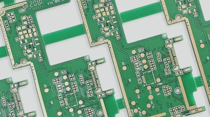
PCB Copper Deposition Process in PCB Manufacturing Technology
In PCB manufacturing technology, the PCB copper deposition process plays a crucial role. The primary purpose of PCB copper deposition is to apply a uniform conductive layer to the walls of non-plated through-holes (NPTH) in 2-layer and multi-layer PCB circuit boards through a redox reaction. This layer is then thickened by electroplating to create plated through-holes (PTH), ensuring the necessary circuit functionality. To achieve this, it is vital to select a stable and reliable chemical copper deposition solution and develop a correct, feasible, and effective PCB manufacturing process.
Challenges and Solutions in Chemical Copper Deposition
Chemical copper deposition is commonly used in plastic electroplating due to its cost-effectiveness, simplicity, and lack of heating requirements. However, this method has its drawbacks, such as poor stability and low deposition rates. Maintaining the stability of chemical copper deposition poses a significant challenge. The reaction can occur not only on activated non-metallic surfaces but also within the solution itself, leading to decreased effectiveness. To address this issue, several methods can be implemented:
- Increasing the stability of the copper ion complex by elevating the concentration of the complex or utilizing strong complexing agents like EDTA, tetramethylene pentamidine, or trimethylene tetramine.
- Reducing the PCB loading.
- Introducing stabilizers such as disulfide compounds or thiol sodium.
- Implementing successive filtration of the solution to prevent autocatalytic action by eliminating solid metal impurities.
- Utilizing air mixing to accelerate the stacking speed and control the self-healing response of copper in the solution.
- Emphasizing stability over speed in stabilizing the electroless copper plating method, as optimizing stacking speed and ensuring stability often present conflicting objectives. Neglecting stability can lead to significant losses.