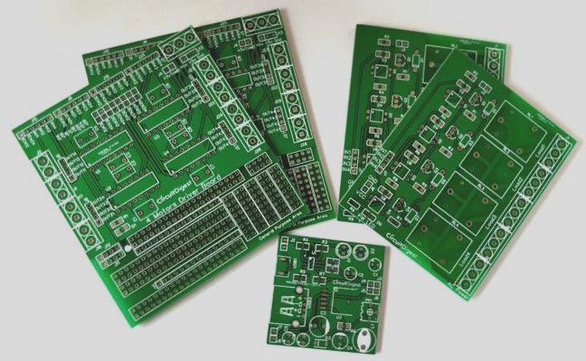
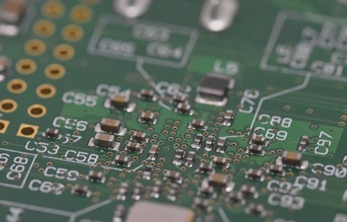
Non-Electrolytic Nickel Coating on PCB Boards: Functions and Requirements
Non-electrolytic nickel coating on PCB boards serves multiple crucial functions, one of which is to facilitate the deposition of gold on the surface. The primary goal of this coating is to establish a robust physical and electrically conductive connection between the PCB board and its components.
Preventing Solder Connection Issues
Modern weak fluxes may fail to create the desired solder connection if the PCB surface contains oxides or contaminants. To ensure successful soldering, the nickel coating must remain free of oxidation to allow gold precipitation.
Importance of Hardness in Electroless Nickel Coatings
Hardness plays a vital role in electroless nickel-coated surfaces, especially in applications requiring physical strength like automotive transmission bearings. While PCB board requirements are less stringent, stiffness is crucial for wire bonding, touch pad contact points, edge connectors, and overall handling sustainability.
Impact on Wire Bonding
Wire bonding necessitates a specific nickel hardness to prevent lead deformation and friction loss, which could lead to the lead “melting” onto the substrate. SEM images have shown no penetration into planar nickel/gold or nickel/palladium/gold surfaces.
Role of Copper and Gold in Circuit Formation
Copper is the preferred metal for circuit formation due to its ease of fabrication and excellent electrical conductivity. Gold, with its good electrical conductivity, is ideal for outer metal layers. While the nickel layer typically doesn’t affect most production boards’ electrical properties, it can impact high-frequency signal transmission, leading to signal losses on microwave PCBs.
Addressing Contact Resistance
Contact resistance is crucial for maintaining conductivity to external contacts, especially after prolonged environmental exposure. Studies have shown varying nickel requirements for different end-use environments to prevent nickel/gold transfer on PCB boards as temperatures increase.