What Is Solder Mask on a PCB?
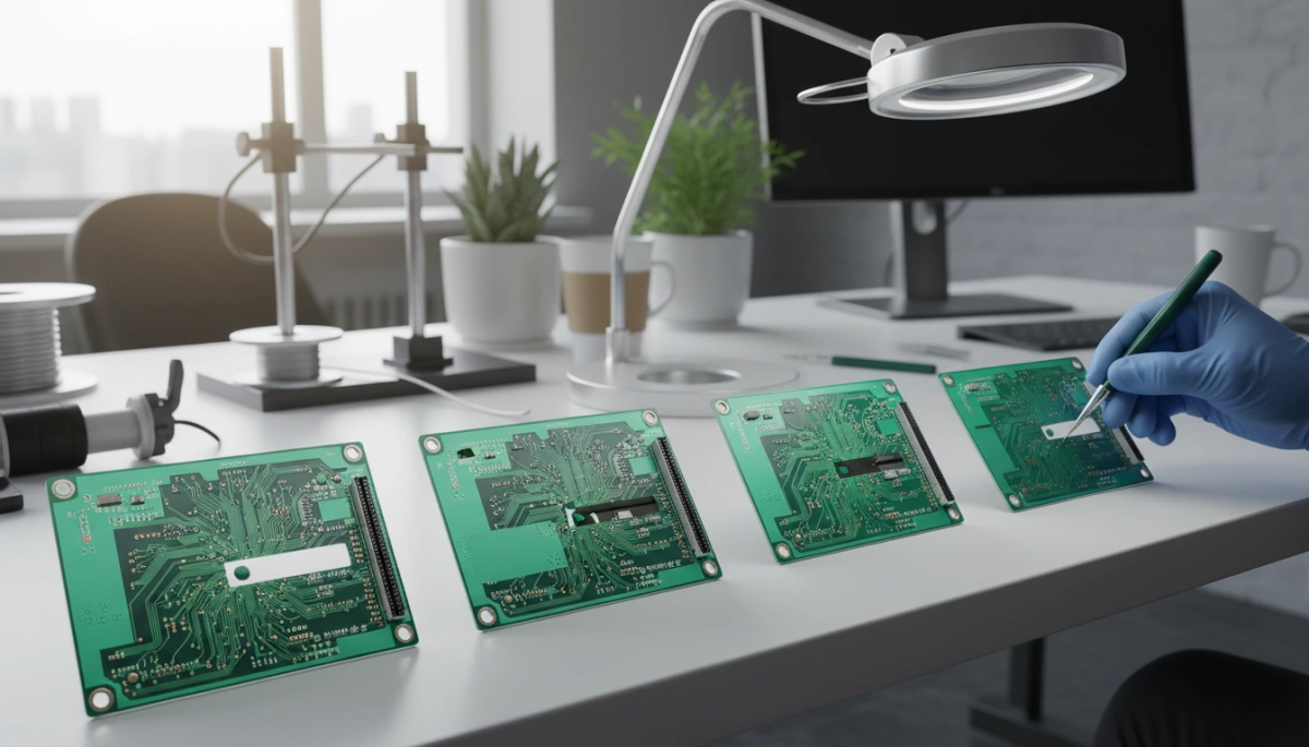
As a PCB designer and manufacturer, I treat solder mask as non‑negotiable on almost every board we build. It’s the thin, colored polymer layer you see covering the copper on a PCB — usually green, but it can be black, red, blue, white, and more.
In simple terms, solder mask (often called solder resist or soldering mask) is a protective coating that sits on top of the copper traces, leaving only specific solder mask openings around pads, holes, and test points where solder actually needs to touch copper.
How Solder Mask Works as a Protective Coating
A modern solder mask PCB uses a liquid or film solder mask ink that’s applied, imaged with UV light, developed, and cured. Once cured, this layer:
- Blocks solder from flowing onto unwanted copper
- Insulates and protects traces from the environment
- Adds a defined boundary around pads and components
In practice, the fabricator controls solder mask expansion (how much larger the opening is than the copper pad) and minimum solder mask sliver (web width) between pads so the mask is manufacturable and doesn’t peel, break, or misregister.
Main Functions of Solder Mask on a PCB
When I decide solder mask rules for a design, I’m thinking about these core functions:
- Stop solder bridges
- Prevents solder from accidentally connecting adjacent pads or traces during reflow or hand soldering
- Critical for fine‑pitch ICs, BGAs, QFNs, and HDI PCB solder mask design
- Protect exposed copper
- Shields copper from oxidation, corrosion, and contamination
- Reduces risk of shorts from stray metal, dust, or tools
- Provide electrical insulation
- Adds a thin dielectric layer over copper
- Helps increase creepage and clearance in tight areas, especially in power electronics and high‑voltage designs
- Improve appearance and readability
- Makes the board look clean and professional
- Enhances contrast between silkscreen and solder mask for easier inspection, debug, and rework
- Supports branding and product differentiation with custom colors
Where You See Solder Mask in Real Products
You’ve seen solder mask PCB technology on almost every product around you:
- Consumer electronics – phones, laptops, game consoles, wearables
- Automotive electronics – ECUs, sensor modules, LED lighting boards
- Industrial controls – PLCs, motor drivers, power supplies
- Networking and high‑speed boards – routers, switches, server backplanes
- LED PCBs – often with white solder mask for LED PCB assemblies to boost light reflection
Anywhere there’s a modern PCB with surface‑mount components and reflow soldering, there’s almost always solder mask.
When Solder Mask Is Optional vs. Mandatory
There are cases where you can skip solder mask — but they’re rare and specific. From a manufacturing and reliability standpoint, I look at it this way:
Solder mask is optional for:
- Very simple, single‑sided, low‑density boards
- Prototypes or test coupons where cost and speed matter more than reliability
- Some RF or analog experiments where bare copper and no mask are intentionally chosen for specific tuning and quick rework
Solder mask is absolutely necessary for:
- Any fine‑pitch SMD design or BGA PCB
- Reflow soldering with solder paste stencils
- HDI PCB solder mask with dense routing and microvias
- High‑reliability, automotive, aerospace, or medical electronics
- Boards that will see moisture, dirt, vibration, or mechanical handling
On real production builds, especially in the US market where quality expectations are high, I strongly recommend treating solder mask as standard, not optional.
Solder Mask vs. No Solder Mask: Reliability, Yield, and Cost
Skipping solder mask might look cheaper at first, but the trade‑offs almost always hit you later. Here’s how I think about it:
With solder mask:
- Higher assembly yield
- Less solder bridging
- More consistent solder joints, especially around fine‑pitch pads and vias
- Better long‑term reliability
- Copper is protected from oxidation and contamination
- Less risk of shorts from debris or handling damage
- More stable process control
- Predictable solder mask opening and solder mask clearance
- Better control over solder spread and joint shape
Without solder mask:
- Higher risk of defects
- Solder can freely flow across copper, causing unintended connections
- Rework time and scrap rate rise, especially in dense areas
- Lower initial PCB cost, higher total cost
- You may save a bit per bare board
- But lose far more in assembly yield, debug time, and field failures
For any serious product — especially something you plan to ship at volume or stand behind as a brand — using a proper solder mask material and process is one of the easiest wins for reliability and professional quality.
Types of solder mask on a PCB
Epoxy liquid solder mask
Epoxy liquid solder mask is the old-school, low-cost option you still see on simple boards and budget runs.
- Best for: low-layer-count PCBs, hobby projects, cost-driven consumer products
- Pros: cheap, decent protection, works fine for wide traces and big pads
- Cons: not great for fine pitch, weaker solder mask registration accuracy, more variation in solder mask thickness
If you’re building a basic controller board or a simple through-hole design, epoxy liquid solder mask still makes sense when every cent matters.
LPI solder mask (liquid photoimageable)
Liquid photoimageable (LPI) solder mask is the modern standard for almost every PCB fab in the US.
- Best for: most commercial and industrial PCBs
- Pros:
- Tight solder mask expansion and minimum solder mask sliver
- Good for fine-pitch SMD, BGA pads, and HDI boards
- Reliable UV curing solder mask ink with strong adhesion and durability
- Typical use: green LPI solder mask on 4–10 layer boards, reflow assemblies, controlled impedance designs
If you’re sending a new design to a US PCB house and don’t know what to pick, LPI solder mask is usually the right move.
Dry film solder mask (DFSM) for HDI
Dry film solder mask (DFSM) is used where you need very fine-line solder mask and tight features.
- Best for: HDI PCB solder mask, microvias, very dense BGA layouts
- Pros: sharper edges, better control of solder mask web width, good for fine pitch solder mask design
- Cons: higher cost, not necessary for normal spacing
If you’re pushing routing limits with heavy BGA use or advanced HDI, DFSM is worth asking your fab about.
Peelable solder mask
Peelable solder mask is a temporary soldering mask designed to be removed after assembly.
- Best for:
- Protecting test pads or gold fingers during reflow soldering or wave solder
- Blocking solder from certain areas in multi-pass assembly
- Pros: easy to peel off, shields areas from flux and solder
- Cons: not a permanent coating, adds a process step
I use peelable solder mask when we need clean connector edges or test pads after aggressive soldering processes.
UV-curable solder mask inks
UV solder mask and UV curing solder mask ink are great for repair, rework, and prototyping in the lab.
- Best for:
- Solder mask repair (covering exposed copper)
- Small-batch prototype PCB fixes
- Pros: quick cure under solder mask UV light, easy to apply by hand
- Cons: not as uniform or controlled as full fab-applied mask
If you ever need to remove solder mask and then re-cover an area, a UV-curable solder mask ink pen is usually the easiest solution.
How to choose the right solder mask type
Here’s a simple way to pick a solder mask PCB option:
- For most US production boards:
→ LPI solder mask (green) – best balance of cost, reliability, and capability - For ultra-dense HDI / fine pitch:
→ Ask your fab about dry film solder mask and their fine-line solder mask specs - For low-cost, simple designs:
→ Epoxy liquid solder mask may be enough if your spacing is relaxed - For temporary protection:
→ Peelable solder mask on connectors, test pads, and no-solder zones - For lab work and fixes:
→ UV-curable solder mask ink for quick repairs and small updates
When in doubt, I always check my PCB manufacturer’s solder mask design guidelines and confirm solder mask material, thickness range, and process before locking in the board stackup.
Solder mask colors and finishes
Common PCB solder mask colors
On most PCB runs in the U.S., I see a few solder mask PCB color standards over and over:
- Green solder mask (gloss or matte) – industry default, best overall balance
- Black solder mask – clean, premium look, popular for consumer and audio gear
- Blue solder mask – common for dev boards and prototypes
- Red solder mask – good contrast, often used for “special” or limited runs
- White solder mask – used a lot for LED PCBs, lighting, and display backplanes
- Matte finishes (green/black) – cut down reflections, look higher-end on small runs
All of these are available in standard LPI solder mask inks from most U.S.-focused PCB fabs.
Why green solder mask is still the default
I still recommend green solder mask for most production designs because:
- It gives best contrast for copper pads, silkscreen, and solder joints
- It works well with AOI and X-ray inspection tuning at most contract manufacturers
- The chemistry is mature, stable, and lower risk for solder mask defects
- It usually has better pricing and lead time than niche colors
If you don’t have a strong branding reason, green is the safest, most reliable choice.
How solder mask color affects inspection and rework
Solder mask color directly impacts inspection, contrast, and rework:
- Green / Red / Blue:
- Good pad and trace visibility
- Easier manual inspection and microscope work
- Black solder mask:
- Low contrast; hard to see hairline bridges or cracks
- Tougher for rework technicians, especially under normal shop lighting
- White solder mask:
- Can stain and discolor after reflow
- Fine details and thin traces are harder to see
If you expect a lot of debug, rework, or field repair, avoid black and pure white unless you really need them.
Heat, light, and LED or camera PCBs
Solder mask color changes heat reflection and light absorption, which matters a lot for:
- LED PCBs / light bars / signage:
- White solder mask reflects light, improves brightness and uniformity
- Green/black can absorb light and create uneven output
- Camera boards / image sensors:
- Black solder mask reduces reflections and stray light
- Helps with image quality and contrast in optical paths
- High-power designs:
- Dark masks run slightly warmer; not huge, but it stacks with other thermal factors
For U.S. lighting products, I nearly always push white mask; for camera modules, I push black around the sensor zone.
Branding and custom solder mask colors
If you’re building a U.S. consumer product, branding with solder mask color can be worth it:
- Pick a custom corporate color (e.g., dark blue or matte black) for visible PCBs
- Use contrasting silkscreen (white on dark, black on light) so text stays readable
- Keep prototype boards green, and move to custom colors once the design is stable
Just remember: custom colors can mean higher MOQs, longer lead times, and tighter DFM discussions with your PCB fab.
When to avoid certain solder mask colors
For high-density or high-heat PCB designs, some solder mask colors are a bad fit:
- Avoid black solder mask on:
- Very fine-pitch BGAs and HDI where you need to visually inspect solder mask slivers
- High-load power boards where every bit of thermal margin counts
- Be careful with white solder mask on:
- High-density routing where contrast is critical
- Boards that will see frequent rework or handling (staining, discoloration)
- Avoid unusual colors if your CM’s AOI profiles are tuned primarily for green
If reliability, yield, and fast debug matter more than looks, default to green LPI solder mask and only customize color where it clearly helps the product.
How solder mask is applied in PCB manufacturing
When I spec a solder mask PCB for US customers, I care a lot about how the fab applies the mask. The process directly affects reliability, rework, and yield.
Surface prep before solder mask
Good solder mask adhesion starts with clean copper:
- Mechanical cleaning: brushing or micro‑etch to roughen copper slightly
- Chemical cleaning: degreasing and oxide removal
- Drying: no moisture or fingerprints before solder mask ink hits the board
If this step is weak, you’ll see solder mask peeling, bubbles, and poor insulation later.
Solder mask application methods
Fabs pick the method based on volume, cost, and line width:
| Method | Typical Use Case | Notes |
|---|---|---|
| Screen printing | Simple, low-cost boards | Thicker, less precise |
| Spraying | Mixed‑tech, medium density | Good coverage, flexible |
| Curtain coating | High volume production | Very uniform thickness |
| Lamination (DFSM) | Dry film solder mask for HDI/fine pitch | Sharp edges, tight solder mask clearance |
Most modern US fabs use LPI solder mask (liquid photoimageable) with spray or curtain coat.
Photoimageable solder mask & UV exposure
For LPI solder mask and UV solder mask:
- Board is coated with liquid mask
- Photo tool / direct imaging defines the solder mask openings
- UV exposure hardens (polymerizes) the exposed areas
- Development washes away unexposed ink, revealing pads and vias
This step controls solder mask registration, solder mask web width, and minimum solder mask sliver between pads.
Curing: thermal or UV
After developing, fabs fully cure the mask:
- Thermal curing: oven bake for maximum durability and adhesion
- UV curing solder mask ink: faster, used in some repair and prototype flows
- Some lines use combined UV + thermal for high‑reliability work
Under‑cure = weak solder mask adhesion and chemical attack. Over‑cure = brittle mask that can crack under thermal cycling.
Top vs bottom solder mask processing
Top and bottom are usually processed the same, but fabs may:
- Cure one side before coating the other to avoid sticking
- Use different solder mask thickness or color for special builds (e.g., white solder mask for LED PCB on one side)
- Adjust exposure/registration based on copper density and warpage
For tight BGA pads and fine pitch, the top side often gets more process attention.
Solder mask quality control
Before a panel ships, a good fab will check:
- Registration: mask aligned to pads, vias, and copper
- Coverage: no exposed copper where mask should be
- Defects:
- pinholes
- blisters/bubbles
- scratches
- missing or narrowed solder mask slivers
- Thickness vs spec (often per IPC-SM-840)
For US customers, I always ask fabs for their solder mask capability table:
minimum solder mask web width, alignment tolerance, and supported solder mask PCB colors (green solder mask, black solder mask, etc.). That’s what keeps reflow and rework predictable.
Solder mask design basics
When I’m setting up a new PCB, solder mask design is one of the first DFM checks I lock in. Good solder mask PCB rules directly impact yield, soldering quality, and rework time.
What is a solder mask opening?
A solder mask opening is the cleared area in the solder mask layer where copper is intentionally exposed for soldering.
You’ll create mask openings for things like:
- Component pads (SMD and through-hole)
- Test pads and probe points
- Certain vias (if you don’t tent or plug them)
Every pad you want soldered must have a solder mask opening. If the mask overlaps the pad by mistake, you’ll get poor wetting or no solder at all.
Solder mask expansion in your PCB CAD tool
In CAD (Altium, KiCad, Eagle, etc.), you control a solder mask expansion value around each pad. That’s how much bigger the mask opening is than the copper pad.
Typical settings for U.S. PCB fabs:
- Standard expansion: +0.002″ to +0.004″ (+0.05 mm to +0.10 mm)
- Fine-pitch / HDI: as tight as +0.001″ (+0.025 mm), but check your fab’s capabilities
Key tips:
- Use your fab’s default solder mask expansion unless you have a strong reason not to.
- Don’t set expansion to zero; real-world solder mask registration isn’t perfect, so you need margin.
- For BGA pads and fine-pitch parts, coordinate values with your CM (contract manufacturer).
Solder mask web (dam) width
The solder mask web (also called solder mask dam or sliver) is the thin strip of mask between two adjacent pads or copper features.
Why it matters:
- It prevents solder bridges during reflow.
- It helps control paste spread and solder joint shape.
Common U.S. manufacturer numbers:
- Minimum solder mask sliver: 0.003″–0.004″ (0.075–0.10 mm) for mainstream fabs
- High-end HDI fabs: can go smaller, but cost goes up
If the web gets too thin, the fab might:
- Drop the dam entirely (mask cleared between pads)
- Or widen clearances, which can change how the board assembles
Balancing manufacturability and density
I always treat solder mask clearance as a trade-off between density and yield:
- More clearance / bigger openings
- Easier for the fab to hit registration
- Less chance of mask partially covering pads
- Slightly higher risk of solder bridges if pads are close
- Tighter solder mask clearances
- Better isolation between close pads
- Needed for fine-pitch BGA and dense designs
- Higher risk of mask defects and lower yield if you push too far
Best practice for U.S. builds:
- Start with your fab’s recommended mask expansion and minimum web width.
- Only tighten where density demands it (BGAs, QFNs, high-pin-count connectors).
- Run DRC with solder mask sliver rules turned on, and fix violations early.
Solder mask vs stencil and solder paste printing
Solder mask design directly impacts stencil design and solder paste printing:
- A well-defined solder mask opening supports the stencil aperture, keeping paste where it belongs.
- If the mask opening is too small or misaligned:
- Paste can smear on mask instead of pad
- You get tombstoning, insufficient solder, or cold joints
- If solder mask dams are missing between fine-pitch pads:
- Paste can bridge during reflow
- You’ll see more shorts under BGAs and QFNs
Simple rules:
- Make sure stencil apertures fit fully inside solder mask openings.
- For fine-pitch parts, involve your stencil house and CM early.
- Never ignore DRC warnings around solder mask clearance, mask to paste, and silkscreen clipped by solder mask.
Dialing in solder mask expansion, mask web width, and clearances is one of the fastest ways to improve reliability and reduce rework on U.S.-built boards.
Solder mask defined vs non-solder mask defined pads
When you’re dialing in solder mask on a PCB, the big choice is NSMD vs SMD pads. This decision directly hits yield, reliability, and manufacturability, especially on BGA and fine‑pitch parts.
What are NSMD (non-solder mask defined) pads?
With NSMD pads, the solder mask opening is larger than the copper pad.
- Copper land: Defines the pad size.
- Solder mask opening: Has a positive solder mask expansion (mask pulled back from the pad).
- Result: You get exposed copper + a bit of surrounding laminate, so solder can “wrap” around the copper edge.
Why designers in the U.S. like NSMD pads:
- Better solder joint reliability (solder wets the pad edges).
- Tighter pad-to-pad tolerance (copper is controlled more accurately than mask).
- Easier rework and inspection on BGA pads.
What are SMD (solder mask defined) pads?
With SMD pads, the solder mask opening is smaller than the copper pad.
- Copper land: Larger than the final exposed area.
- Solder mask: Overlaps the pad, so the mask edge defines the pad.
- You get a negative solder mask expansion (mask overlaps copper).
What this gives you:
- More support around the pad (mask acts like a mechanical “collar”).
- Slightly flatter, more controlled solder joint shape.
- Better in some fine-pitch BGA cases where you need tight solder mask web (sliver) between pads.
When to use NSMD pads for better reliability
I default to NSMD pads for most BGA pads and SMT pads on standard boards:
- When you want strong, reliable solder joints.
- When your PCB fab can hold tight copper tolerances.
- For reballing, rework, and X-ray inspection — NSMD is easier to handle.
- Typical use: Consumer electronics, industrial, and most reflow soldering builds.
Rule of thumb: If your BGA pitch is not extreme (≥ 0.5 mm) and your fab is competent, go NSMD.
When SMD pads make sense for BGAs and fine-pitch
SMD pads start to make sense when pitch gets very tight and solder mask web width is critical:
- Very fine-pitch BGAs (0.4 mm and below).
- Where minimum solder mask sliver (mask web between pads) is close to the fab’s limit.
- Designs that need extra pad stability, like some high-density smartphone/tablet style PCBs.
- When your assembly house wants to really control solder volume and avoid bridging.
Trade-off: SMD helps with spacing and stability but can slightly reduce solder joint fatigue performance compared to NSMD.
Impact on pad size, copper land, and solder joint shape
NSMD pads:
- Copper pad smaller than the mask opening.
- Solder flows around the edge of the copper, giving a more filleted, rounded joint.
- Better thermal cycling performance and stress relief.
SMD pads:
- Copper pad larger, mask cuts into it.
- Exposed area is smaller, with sharper boundaries.
- Solder joint is more “contained” and flat, which can help reduce bridging on ultra‑fine pitch.
DFM tips for choosing SMD vs NSMD with your PCB fab
Before locking in your solder mask PCB rules, talk to your fab in the U.S. market terms they’re used to:
- Ask for their standard solder mask expansion and minimum solder mask sliver:
- Typical mask expansion: +2 to +5 mil (0.05–0.125 mm) for NSMD.
- Typical minimum mask web: 3–4 mil (0.075–0.1 mm).
- Share your BGA pitch and solder mask defined pad strategy early.
- Confirm:
- Their solder mask registration capability (how well mask lines up with copper).
- Supported LPI solder mask specs and colors (green solder mask is usually the cleanest for yield).
- For fine-pitch BGAs:
- Have the fab review Gerbers and your solder mask openings before release.
- Be open to switching some pads to SMD per their DFM feedback.
If you’re unsure, set NSMD as default, then use SMD pads only where the fab says it’s necessary to meet their solder mask clearance and web width limits.
Solder mask clearances and rules of thumb
When I’m setting up solder mask on a PCB, I keep a few simple rules so the fab doesn’t push back, and the boards don’t get expensive.
Typical solder mask expansion values
For standard US PCB processes, these solder mask expansion numbers work well for most designs:
- Standard mask expansion (solder mask opening around pads):
- +3–4 mil (0.075–0.1 mm) per side for normal SMT pads
- +2 mil (0.05 mm) per side for finer-pitch work (talk to your fab first)
- Use global solder mask expansion rules in your CAD, then only override on special pads (like BGA pads or via-in-pad).
Minimum solder mask sliver (web width)
That thin strip of solder mask between pads is your solder mask sliver (or web). If it’s too thin, it breaks or disappears in fab.
- Safe rule for most low–mid cost fabs:
- ≥ 4 mil (0.1 mm) minimum solder mask web width
- Tighter HDI / high-end fabs:
- 3 mil (0.075 mm) is often okay, some can go a bit lower, but cost goes up.
- If the minimum solder mask sliver is below your fab’s limit, they’ll either merge openings or ask you to relax the design.
Solder mask spacing around pads, vias, and copper
To keep solder mask registration issues from causing shorts:
- Keep mask clearance around copper (traces, copper pours):
- At least 2–3 mil (0.05–0.075 mm) away from exposed copper unless it’s intentional.
- Vias:
- Tented vias (covered with solder mask): Okay for small signal vias.
- Open vias: Give them their own mask opening, or group them, but avoid half-covered “donut” openings.
- Avoid tiny mask islands between a via and pad; remove them or increase spacing.
Silkscreen to solder mask clearance
Silkscreen that lands on bare copper or pads is a mess in assembly. Mask controls where silkscreen can actually survive.
- Silkscreen to solder mask clearance:
- Keep ≥ 4–5 mil (0.1–0.125 mm) from any exposed pad opening.
- Most fabs will clip silkscreen that overlaps a solder mask opening. That’s why you’ll see silkscreen clipped by solder mask on your review images.
- Make text at least 40 mil (1 mm) height for good readability in real production.
Common DRC rules for solder mask in CAD tools
In tools like Altium, KiCad, and Fusion 360, I usually set:
- Solder mask expansion: global value (+3–4 mil)
- Minimum solder mask sliver / web width: 4 mil
- Clearance between solder mask and copper: 2–3 mil
- Silk to solder mask clearance: 4–5 mil
- Separate rules for BGA pads, via-in-pad, and fine pitch footprints.
Always pull your fab’s PCB solder mask design guidelines and plug those straight into your DRC rules.
How tighter solder mask clearances affect yield, cost, and lead time
Pushing “hero” numbers on solder mask clearance is almost never free:
- Tighter mask expansion and smaller slivers:
- Higher risk of solder mask defects (breaks, missing dams, mis-registration)
- More solder bridging between fine-pitch pads
- Lower yield, so fabs charge more or push out lead times
- Looser, more forgiving solder mask rules:
- Better reliability and repeatability in US production
- Faster DFM approval and fewer surprises during assembly
- Lower risk of needing solder mask repair or re-spin
If you’re not doing bleeding-edge HDI, it’s smarter in the US market to keep solder mask expansion and minimum solder mask sliver conservative and let the assembly line run smoother and cheaper.
Via and solder mask strategies
When I’m setting up a PCB solder mask, I treat vias as a reliability and assembly problem first, not just a cosmetic one. The way you combine vias with solder mask (tented, open, plugged, via-in-pad) will decide how clean your reflow is and how often your CM calls you with problems.
Tented vias with solder mask
Tented vias are vias fully covered by solder mask on one or both sides.
They’re a good idea when:
- You want to prevent solder wicking during reflow
- You don’t care about probing those vias in test
- You want better protection against oxidation and contamination
Typical PCB CAD settings:
- Mark small vias as “tented” or “covered” in the via properties
- Use a solder mask expansion of 0 mil (or slightly negative) so the via pad is fully under the mask
Plugged and capped vias
For higher reliability designs, I usually recommend plugged and capped vias:
- Plugged vias: hole filled (usually with epoxy or conductive fill), then covered with solder mask
- Capped vias: filled and then plated over (common in HDI and via-in-pad)
Why use them:
- Better thermal and mechanical reliability
- No solder wicking through via holes
- Cleaner BGA pads and flat surfaces for assembly
Ask your PCB fab for:
- Their via plug/cap process, compatible hole sizes, and cost adder
- IPC-compliant options for via filling and solder mask coverage
Open vias and solder wicking
Open vias (solder mask opening over the via pad and hole) are cheaper but risky in assembly:
Problems you’ll see:
- Solder wicks down via holes, starving nearby pads
- Uneven solder joints under BGAs and fine-pitch parts
- Random solder balls on the bottom side after reflow
Where open vias are acceptable:
- Low-cost prototypes and hobby boards
- Non-critical signals away from component pads
If you must leave them open:
- Keep them away from pads that see solder paste
- Use a smaller copper pad and tighter solder mask clearance when your fab can hold it
Via-in-pad with solder mask and fill
Via-in-pad is standard for fine-pitch BGA and HDI PCB designs in the US market, but only if done correctly:
Best practice:
- Filled and capped via-in-pad (via filled, then plated, then solder mask defined opening)
- Flat, stable pads that won’t suck solder away during reflow
- Essential for 0.5 mm pitch and smaller BGA pads
Avoid:
- Raw, open via-in-pad with just solder mask over the hole (you’ll get voided or starved joints)
Coordinate with your fab on:
- Via fill type (non-conductive / conductive)
- Solder mask defined pads vs non-solder mask defined pads (NSMD) for BGA land patterns
Solder mask over vias and reflow behavior
How solder mask covers vias directly affects reflow:
- Tented vias: less solder wicking, fewer solder balls, better cleanliness
- Partially covered vias (poor solder mask registration): can cause odd solder icicles or bridges
- Plugged + capped vias: best behavior in reflow, especially under BGAs and power packages
For high-speed and high-current designs, I lean toward:
- Filled + capped vias under critical pads
- Proper solder mask opening control to keep reflow repeatable
Setting via solder mask options in your CAD tool
In your PCB CAD (Altium, KiCad, Eagle, etc.), set via solder mask rules intentionally, not by default:
- Create specific rules for:
- Tented vias (small signal vias)
- Open vias (test points, thermal relief vias where needed)
- Via-in-pad (filled, capped, BGA-specific rules)
- Control:
- Solder mask expansion for vias
- Minimum solder mask sliver/web width between via pads and component pads
- Always review:
- The solder mask layer in a Gerber viewer
- That vias near pads aren’t accidentally sharing one big solder mask opening
If you’re building in the US or using US-focused assembly houses, getting these via and solder mask strategies right will save you from false opens, BGA rework, and painful debug later.
Solder mask thickness and material properties
When I’m reviewing PCB stackups for U.S. customers, solder mask thickness and material choice are a bigger deal than most people expect—especially once you get into high‑speed, RF, or tight‑impedance work.
Typical solder mask thickness ranges
On a standard LPI (liquid photoimageable) solder mask PCB, you’ll usually see:
- Over copper: ~0.4–0.8 mil (10–20 μm) cured
- Over bare laminate: ~0.6–1.2 mil (15–30 μm) cured
- Dry film solder mask (DFSM): often 0.8–1.6 mil (20–40 μm)
Fabs measure solder mask thickness with:
- Microsection cross‑sections (IPC method)
- Non‑contact gauges for process control
If you don’t call it out, I assume a normal LPI solder mask thickness per my fab’s default IPC-SM-840 class.
How solder mask thickness affects impedance and SI
For general digital boards, the mask’s impact on impedance is small. Once you’re in 5+ Gbps, RF, or tight 50/90 Ω control, it can matter:
- Thicker solder mask = higher effective dielectric constant around the trace
→ slightly lower impedance - Very thin or no solder mask (for RF microstrip)
→ slightly higher impedance, less dielectric loading
On high‑speed PCB designs, I:
- Ask the fab for their actual cured solder mask thickness
- Include it in the field solver model (or specify “no mask” on RF segments)
Dielectric properties vs core/prepreg
Compared with FR-4 core/prepreg:
- Solder mask Dk (dielectric constant): ~3.3–4.0 at 1 GHz
- Core/prepreg Dk: typically 3.8–4.4 (standard FR‑4), lower for high‑speed materials
- Loss tangent (Df) of solder mask: usually higher than controlled‑loss cores
What this means in practice:
- Solder mask sits close to surface microstrip traces, so it slightly changes the local dielectric mix
- It matters most for fine‑line high‑speed and RF traces, less for buried stripline
Solder mask impact on high-speed, RF, and impedance
For high‑speed PCB and RF boards in the U.S. market, I usually recommend:
- Critical RF lines:
- Option A: no solder mask over those traces (local “open” mask area)
- Option B: use a controlled, thin LPI solder mask and model it
- Differential pairs / impedance‑controlled nets:
- Confirm mask thickness and type with the fab
- Avoid random mask “islands” or uneven coverage around the pair
- Fine‑pitch HDI: choose LPI or DFSM with tight solder mask registration and thin, even coating
Thickness, coverage, and ENIG / other finishes
Solder mask and finish (ENIG, HASL, OSP) need to play nice:
- ENIG pads
- Mask defines solder mask opening and keeps nickel/gold only on exposed copper
- Inconsistent mask thickness around pads can change wetting and fillet shape
- Too thick mask at pad edges → step that can trap flux or affect solder paste release
- Too thin / undercured mask → solder mask peeling, poor adhesion, or exposed copper
On ENIG builds, I make sure:
- The fab keeps uniform coating and cures per spec
- Pad‑to‑mask transitions are smooth for clean reflow soldering
IPC standards and spec ranges
Most quality fabs in the U.S. follow IPC-SM-840 for solder mask materials:
- Classes: T (telecom), H (high reliability), etc.
- Defines minimum insulation resistance, adhesion, hardness, thickness ranges, flammability, and thermal cycling performance
- Typical specs call out:
- Minimum cured thickness over copper
- Adhesion and flexibility after thermal shock
- Electrical insulation levels for high‑voltage or high‑reliability work
If your project is automotive, aerospace, or medical, I always:
- Specify IPC-SM-840 Class H or what your QA requires
- Confirm the solder mask material data sheet (Dk, Df, Tg, temp rating, RoHS)
Dialing in solder mask thickness, material, and standards early avoids ugly surprises on impedance, signal integrity, and long‑term reliability.
Solder mask for special PCB types
Solder mask on flexible and rigid-flex PCBs
For flex and rigid-flex PCBs, the solder mask (or coverlay) has to bend without cracking or peeling. I always pick flexible solder mask ink or polyimide coverlay for these builds.
Key points:
- Use flex-specific solder mask materials, not standard rigid LPI
- Avoid full mask coverage on tight bend areas to reduce stress
- Keep solder mask thickness low and uniform so the flex section can move freely
- Confirm with your fab what they support for rigid-flex PCB solder mask
Very thin or flex materials challenges
On very thin cores and flex, solder mask adhesion and registration get tricky.
I watch for:
- Solder mask peeling from too much bend or poor adhesion
- Mask cracking near stiffeners or sharp corners
- Overly aggressive solder mask expansion that creeps into bend zones
- The need for lower bake temps to avoid warping thin material
Solder mask for HDI and microvia boards
HDI, microvias, and fine-pitch BGAs demand tight solder mask clearance and stable registration.
Best practices:
- Use LPI solder mask or dry film solder mask (DFSM) for fine features
- Tight but realistic minimum solder mask sliver (check fab capability—often 3–4 mil for U.S. production)
- Consider solder mask defined pads for very fine-pitch BGA pads if your fab recommends it
- Make sure your CAD rules match the fab’s fine pitch solder mask design guidelines
High-temperature and high-reliability solder mask options
For automotive, industrial, or aerospace work in the U.S., I always spec high-temperature solder mask that meets IPC-SM-840 Class T/H.
What I focus on:
- Proven solder mask adhesion through multiple reflow cycles
- High Tg and good insulation resistance at elevated temps
- Compatibility with your reflow soldering profile and finish (ENIG, immersion silver, etc.)
LED PCBs and white solder mask
For LED PCBs, especially aluminum MCPCBs and light bars, white solder mask is common, but it has trade-offs.
Consider:
- White solder mask improves light reflection, great for brightness
- But white mask can be harder for AOI and manual inspection
- Use high-quality white solder mask for LED PCB to avoid yellowing and poor adhesion
- Keep copper well covered to prevent solder mask defects showing through the light
Power electronics and high-current boards
On power boards and high-current designs, solder mask PCB choices affect both reliability and cooling.
I usually:
- Keep solder mask off high-current copper planes where you need better heat dissipation or heavy solder plating
- Use thicker, robust solder mask around large pads and bus bars to prevent tracking and arcing
- Carefully define solder mask openings around big thermal pads so solder doesn’t flood into unwanted areas
- Confirm creepage/clearance requirements and set solder mask spacing and rules accordingly in CAD
Common solder mask defects and how to fix them
Typical solder mask defects on a PCB
Here are the most common solder mask PCB issues you’ll see in US production and assembly:
- Peeling / poor adhesion
- Causes: dirty copper, bad surface prep, under-cured solder mask ink, wrong bake profile.
- Fix: tighten cleaning (micro-etch, proper rinse), verify solder mask curing process, follow IPC-SM-840 recommendations.
- Pinholes and bubbles
- Causes: trapped air, contamination, too-thick wet film, over-aggressive spray.
- Fix: adjust solder mask application methods (screen printing / spray), improve drying, add in-line inspection for bubbles.
- Misalignment / registration shift
- Causes: poor solder mask registration, bad panel tooling, film stretch, loose process control.
- Fix: improve tooling holes and fiducials, lock down exposure alignment, clarify minimum solder mask sliver / web rules with your fab.
Solder bridging from bad solder mask design
Bad solder mask opening and spacing is a classic cause of shorts in reflow:
- Too small solder mask web width between pads lets mask wash away.
- Over-ambitious pitch on QFNs/BGAs without respecting minimum solder mask sliver.
- Poor paste stencil plus weak mask = bridges everywhere.
To avoid solder bridging:
- Use your fab’s published solder mask clearance and web width limits.
- Don’t “cheat” below ~3–4 mil webs unless your fab explicitly supports fine-line LPI solder mask.
- Validate with DFM before you order boards.
Oxidation or corrosion under solder mask
If you see dark copper or corrosion creeping under the solder mask:
- Likely causes:
- Incomplete cleaning / etch before mask
- Under-cured mask, poor solder mask adhesion
- Aggressive environment (humidity, flux residues, contamination)
- What to push your fab to check:
- Copper cleanliness and micro-etch control
- Mask thickness and full cure (thermal or UV solder mask)
- Compliance with IPC-SM-840 material and process limits
How PCB fabs prevent solder mask defects
Serious US-focused fabs keep solder mask defects low by:
- Tight control of photoimageable solder mask process (exposure, development, cure)
- Automated optical inspection for solder mask registration and coverage
- Test coupons for adhesion, thickness, and cure level
- Clear capability tables for solder mask expansion, web width, and fine-pitch features
When you source boards, ask directly:
- “What’s your minimum solder mask web width?”
- “How do you verify cure for your LPI solder mask or UV curing solder mask ink?”
Solder mask repair and touch-up
For prototypes and small US assembly runs, solder mask repair is normal:
- UV-curable solder mask ink
- Great for quick fixes around pads and vias.
- Apply, level, cure with UV light, then lightly inspect and test for insulation.
- Epoxy-based touch-up
- Good for high-temp or high-reliability spots.
- Takes longer to cure, but tougher under abuse.
If you need to remove solder mask locally:
- Use a fiberglass pen, fine abrasive, or controlled scraping.
- Keep the exposed copper small and re-protect with UV mask or conformal coat.
Cosmetic vs real reliability problems
Not every solder mask PCB flaw means a scrap board:
- Mostly cosmetic (usually OK):
- Color variation between panels
- Tiny mask nicks away from any copper
- Silkscreen clipped by solder mask
- Real reliability risk (reject or rework):
- Exposed copper that should be insulated
- Mask peeling near pads or high-voltage areas
- Pinholes or cracks that can lead to corrosion paths
- Misregistration that changes pad shape on BGA / fine-pitch parts
My rule:
If a solder mask defect can create a short, corrosion, or change the effective pad size, I treat it as a reliability problem, not cosmetics.
Advanced solder mask processes and trends
Solder mask tech is moving fast, and if you’re building boards in the U.S. for high‑reliability or high‑density work, these trends matter for yield, cost, and consistency.
Inkjet-applied solder mask PCB
Inkjet-applied solder mask is becoming a serious option for high‑precision builds:
- Direct imaging: No screens, no films – the solder mask ink is jetted exactly where it’s needed.
- Tighter solder mask expansion and minimum solder mask sliver control for fine‑pitch BGAs and HDI.
- Better registration around pads, vias, and fine traces, which means fewer solder mask defects and less rework.
- Great fit for prototype PCB runs where revisions are frequent.
If you’re pushing fine pitch solder mask design, ask your fab if they support inkjet solder mask or only classic LPI.
Eco-friendly and low-VOC solder mask ink
More U.S. customers care about clean processes and compliance:
- Low-VOC solder mask materials help with OSHA and local air-quality rules.
- Newer LPI solder mask and UV solder mask chemistries cut down on solvents and waste.
- Some fabs now promote eco-friendly solder mask ink as a standard, not a premium.
If you build for medical, industrial, or gov markets, this can be a real selling point.
Fine-line solder mask for HDI PCB
Next‑gen HDI and high‑speed boards need serious fine-line solder mask capability:
- Tighter solder mask clearance around micro BGAs and via-in-pad.
- Smaller solder mask web width between pads and traces without mask breakout.
- Better control for solder mask for BGA pads and non solder mask defined pads on dense designs.
Always match your layout rules to what your fab can really print, not what your CAD tool allows.
Automation and inspection for solder mask quality
High‑end fabs lean hard on automation to keep solder mask PCB quality tight:
- AOI (automated optical inspection) for solder mask registration, pinholes, and mask encroaching on pads.
- Inline measurement of solder mask thickness and coverage.
- Logged process data for solder mask curing, adhesion, and consistency from lot to lot.
This reduces solder mask peeling, misalignment, and random yield hits during reflow soldering.
Low-cost vs high-end fab solder mask capabilities
Not all PCB shops are equal when it comes to solder mask:
Typical low-cost fab limits:
- Larger solder mask expansion and minimum solder mask sliver.
- Looser solder mask registration around pads.
- Fewer color options and older LPI processes.
- Less consistent solder mask thickness and curing.
High-end fab strengths:
- Reliable fine pitch solder mask design for HDI and BGA.
- Better rigid-flex PCB solder mask options and high-temp mask for power or automotive.
- Advanced materials that behave better on high speed PCB and RF boards.
- Stricter IPC-SM-840 compliance and lot documentation.
What to ask your PCB manufacturer about solder mask
When I source boards or qualify a new shop, I’m direct about solder mask. Here’s what I always ask:
- What solder mask materials and colors do you support? (Ask for data sheets and IPC-SM-840 class.)
- What are your standard and minimum solder mask expansion and sliver? (In mils.)
- Do you offer inkjet-applied or only standard LPI solder mask?
- What’s your typical solder mask thickness range? Top vs bottom.
- How do you control and inspect solder mask registration and defects?
- What’s your process for tented vias, plugged vias, and via-in-pad with solder mask?
- Do you support low-VOC or eco-friendly solder mask options?
These questions tell you fast whether a fab is set up for basic hobby boards or serious production work in the U.S. market.
Practical solder mask PCB tips
Set up solder mask rules in your CAD
I always lock in solder mask rules early in the design so I don’t fight DRC at the end.
Key defaults (check with your PCB fab’s stackup notes):
- Solder mask expansion (mask opening around pads):
- Standard boards: +3–5 mil (0.075–0.125 mm)
- Fine‑pitch / BGA: +2–3 mil
- Minimum solder mask sliver / web width (mask between pads):
- Low‑cost fabs: 4–5 mil min
- HDI fabs: 2–3 mil min
- Via options (per-net or global):
- Tented vias for dense areas and BGAs
- Open vias for test pads and grounding, with enough solder mask clearance
- Separate rules for solder mask defined pads (SMD) and non solder mask defined pads (NSMD), especially on BGA pads.
Set these in your design rules / constraints so the tool auto-enforces your solder mask openings and clearances.
Check solder mask layers in Gerber tools
Before I send a board out, I always sanity-check the solder mask Gerber files:
- Load Top/Bottom solder mask layers with copper and paste in a viewer (e.g., Gerbv, KiCad’s viewer, GerberLogix, or your fab’s online viewer).
- Confirm:
- All pads have proper solder mask openings
- BGA pads aren’t accidentally merged by missing mask webs
- Vias are correctly tented / open / plugged based on settings
- No silkscreen clipped by solder mask in critical areas
- Zoom in on:
- Fine‑pitch ICs, BGAs, and connectors
- Tight areas where minimum solder mask sliver might be violated
Catching a bad solder mask sliver or wrong via mask here saves a full respin.
Use your PCB fab’s solder mask guidelines
For U.S. builds, I always design to the fab’s real capabilities, not a generic app note.
Ask your fab (or check their website) for:
- Minimum solder mask web width
- Standard solder mask thickness and material (LPI, UV solder mask, etc.)
- Supported solder mask colors and their impact on cost/lead time
- Recommended solder mask expansion for:
- Fine-pitch
- BGA
- High‑current pads
- Any special rules for rigid‑flex PCB solder mask or HDI PCB solder mask
Then mirror those numbers into your CAD rules so you’re DFM‑clean from day one.
Common solder mask PCB mistakes
I see the same solder mask mistakes over and over:
- Zero or negative solder mask expansion → mask covers part of the pad, causing bad reflow.
- Ignoring minimum solder mask sliver → merged pads, solder bridges, yield hits.
- Open vias in pads with no fill → solder wicking, starved joints.
- Using white solder mask for LED PCB or camera boards without checking reflectivity and cleanliness issues.
- No silkscreen to solder mask clearance → unreadable text after fab clips silkscreen.
- Forgetting to check solder mask vs paste mask alignments on BGAs.
All of these are avoidable with good rules and a quick Gerber review.
Early DFM review on solder mask
Early DFM with your PCB house is the easiest win for U.S. teams trying to hit schedule and budget:
- Send preliminary Gerbers or screenshots of your dense areas (BGAs, HDI sections).
- Ask them to review:
- Solder mask registration limits and tolerances
- Fine‑pitch solder mask web width capability
- Whether your via-in-pad + mask strategy is buildable with their process
- Let them flag anything that will:
- Increase cost (special solder mask ink, extra steps)
- Cut yield (too tight solder mask clearance, marginal slivers)
- Delay lead time (non‑standard color, special UV curing solder mask ink)
A 20‑minute DFM pass up front usually saves at least one respin and a couple weeks of schedule on production builds.
Solder mask FAQs and quick answers
Solder mask vs paste mask
| Term | What it is | Layer use in CAD |
|---|---|---|
| Solder mask | Protective coating that covers copper | Top/Bottom Solder Mask |
| Paste mask | Openings in the stencil for solder paste | Top/Bottom Paste |
- Solder mask opening = where copper is allowed to be exposed.
- Paste mask = where solder paste is printed for reflow.
- You can have a solder mask opening without paste (test pads), and paste only where you actually place parts.
Typical solder mask thickness
For most US PCB fabs using LPI solder mask PCB processes:
- Standard thickness: 0.7–1.2 mil (≈ 18–30 µm) over copper
- Heavy copper / high-reliability: up to 1.5–2.0 mil
- I usually spec:
- “LPI solder mask, 0.8–1.2 mil finished thickness” unless the fab has a fixed house spec.
Can you remove or repair solder mask?
Remove solder mask (localized):
- Small areas:
- Fiberglass pen, fine sandpaper, or a sharp knife
- Follow with IPA cleaning
- Avoid big bare areas; you’ll invite corrosion and solder bridges.
Solder mask repair:
- Use UV solder mask or UV curing solder mask ink, or 2-part epoxy.
- Steps:
- Clean copper, lightly scuff
- Apply ink/epoxy
- Expose with UV and fully cure
- Works well for solder mask peeling, scratches, and pinholes.
Why green solder mask is still everywhere
- Best contrast for visual inspection and AOI vs copper and silkscreen.
- Mature process: green LPI solder mask has the tightest capabilities and lowest defect rate.
- Cheapest option at almost all US PCB fabs.
- Handles reflow soldering and rework better than many bright or dark colors.
What “minimum solder mask sliver” really means
- Solder mask sliver / web width = the narrow strip of solder mask between two openings.
- Typical fab capabilities in the US:
| Fab class | Minimum solder mask sliver |
|---|---|
| Low-cost / standard | 4–5 mil |
| Mid-range | 3–4 mil |
| HDI / high-end | 2–3 mil (sometimes 2 mil) |
- If you push below their spec, slivers break off, causing unwanted bridges and lower yield.
How solder mask color and type affect assembly and rework
- Color impact:
- Green solder mask: best for AOI, manual inspection, and rework.
- Black solder mask: poor contrast, absorbs heat, harder to see bridges.
- White solder mask (LED PCB): great light reflection, but can stain and be harder for AOI.
- Matte colors: reduce glare, help with camera-based inspection.
- Type impact:
- LPI solder mask: default for reflow, strong adhesion, good solder mask clearance control.
- Dry film solder mask (DFSM): used for fine pitch and HDI, tighter solder mask web width.
- Peelable solder mask: only for temporary masking (wave, selective solder), not permanent.
If you’re building fine-pitch BGA, LEDs, or high-speed boards in the US, I always confirm with the fab:
- Solder mask material,
- Minimum solder mask expansion,
- Minimum solder mask web,
before locking the design.