Complete Guide to Rigid PCB: Design, Manufacturing, and Applications
Introduction
Rigid PCBs (rigid printed circuit boards) are non-flexible electronic interconnection platforms that serve as the structural foundation for approximately 90% of all electronic devices manufactured today. These rigid circuit boards provide essential mechanical support and electrical connectivity for components ranging from simple consumer electronics to complex aerospace systems.
Understanding rigid PCB technology is essential for electronics design and manufacturing because these boards form the backbone of modern electronic products, influencing everything from device reliability to manufacturing costs.
What This Guide Covers
This comprehensive guide covers rigid PCB construction fundamentals, substrate materials and specifications, manufacturing processes, design considerations, and practical applications across various industries. We focus specifically on rigid boards while noting their relationship to flexible circuits and rigid flex designs for context. A flex PCB, or flexible printed circuit board, is a type of flexible board that can be bent, folded, or twisted to fit into compact or irregularly shaped devices, offering advantages in space-saving and durability. A rigid flex PCB combines both rigid and flexible sections in a single board, allowing for complex three-dimensional designs and reliable connections across moving or folding parts—features not possible with standard rigid PCBs.
Who This Is For
This guide is designed for electronics engineers, PCB designers, product developers, and manufacturing professionals working with electronic devices. Whether you’re designing your first printed circuit board or optimizing manufacturing processes for high volume production, you’ll find practical insights for successful rigid PCB implementation.
Why This Matters
Rigid printed circuit boards form the foundation of electronic devices from cell phones and desktop computers to flat screen TVs and solid state drives. Understanding their design principles, material properties, and manufacturing constraints directly impacts product performance, reliability, and assembly costs in today’s competitive electronics market.
What You’ll Learn:
Rigid PCB structure fundamentals and material composition
Layer configurations from single sided PCBs to complex multilayer structures
Manufacturing process steps and material selection criteria
Common design challenges and proven solutions
Understanding Rigid PCB Technology
A rigid PCB is a printed circuit board constructed from inflexible substrate material that cannot bend without damage, typically using FR4 fiberglass as the base material. This FR4 is a common rigid substrate material, providing the stiffness and durability required for demanding electronic applications.
The rigid construction provides dimensional stability and mechanical support that protects delicate copper traces and mounted components from physical stress. Rigid PCBs are built using rigid materials such as fiberglass, which deliver the necessary stiffness and stability to support electronic components without flexing. Unlike flexible PCBs that can bend and flex during operation, rigid boards maintain their shape throughout the product lifecycle, ensuring reliable performance in applications where structural integrity is paramount.
This rigidity matters because it enables secure component mounting, consistent electrical connections, and predictable mechanical behavior under various operating conditions including vibration, thermal cycling, and mechanical stress. The solder mask provides insulation over the copper traces, and manufacturers also add insulation to further prevent electrical damage and ensure safety on the board.
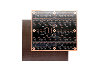
Core Structure and Components
The foundation of any rigid board consists of multiple layers working together to provide both electrical functionality and mechanical strength. On rigid PCBs, different components such as copper traces, conductive pathways, and substrates are assembled to connect and support the overall circuit functionality within the rigid structure. The substrate layer, typically made from FR4 fiberglass material, forms the structural core that gives the board its rigid characteristics and insulation properties.
Copper layers are laminated onto this substrate material to create conductive pathways for electrical signals. The copper foil thickness can range from 0.5 oz to 6 oz depending on current-carrying requirements, with thicker copper providing better current capacity and heat dissipation capabilities.
This relationship between substrate rigidity and copper layer adhesion creates the fundamental structure that enables reliable component mounting and long-term electrical performance in electronic products.
Add Your Heading Text Here
FR4 fiberglass serves as the primary substrate material due to its excellent electrical insulation properties, mechanical strength, and thermal stability. This base material can withstand high temperatures during manufacturing and operation while maintaining dimensional accuracy and low moisture absorption.
The copper layer specifications determine the board’s electrical conductivity characteristics, with standard copper thickness options supporting various current requirements and signal integrity needs. Advanced applications may require specialized conduction material or metal core substrates for enhanced heat dissipation.
Building on this substrate foundation, additional layers including solder mask layer and silkscreen layer complete the rigid PCB structure. The solder mask provides insulation and protection for copper traces, while the silkscreen layer enables component identification and assembly guidance.
Transition: Understanding these fundamental materials and structures enables us to explore how different layer configurations create various rigid PCB types for specific applications.
Types and Configurations of Rigid PCBs
Building on the material understanding established above, rigid printed circuit boards are manufactured in several distinct configurations that balance complexity, cost, and performance requirements. Single board designs, such as single board computers or layouts, integrate multiple functions or components within one compact unit, offering advantages in simplicity and integration compared to multi-board configurations.
Single-Layer Rigid PCBs
Single sided PCBs feature copper traces on only one side of the substrate material, representing the simplest and most cost-effective rigid board configuration. These boards use a single conductive layer to create electrical pathways, with components typically mounted on the non-copper side and connected through holes.
This construction approach minimizes manufacturing complexity and material costs, making single layer boards ideal for basic consumer electronics, toys, and simple control circuits where space constraints and component density are not critical factors.
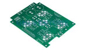
Double-Sided Rigid PCBs
Double sided PCBs incorporate copper layers on both sides of the substrate layer, connected through plated through-holes that enable electrical continuity between the top and bottom surfaces. Unlike single-layer boards, this configuration enables more complex routing options and higher component density within the same board footprint.
The dielectric layers between the two copper surfaces provide electrical isolation while maintaining mechanical rigidity, and through-hole plating creates reliable electrical connections that support more sophisticated circuit designs than single sided alternatives.
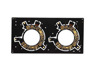
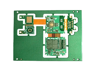
Multi-Layer Rigid PCBs
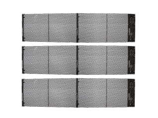
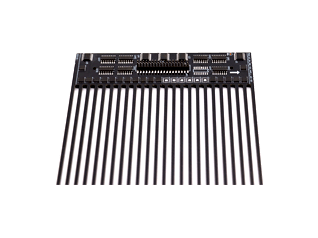
Multi-layer rigid boards contain three or more layers of copper separated by insulating substrate material, enabling complex routing in compact form factors essential for modern electronic devices. These multilayer structures can incorporate 4 to 40+ layers depending on design requirements and manufacturing capabilities.
Advanced applications in computer motherboards, telecommunications equipment, and aerospace systems rely on multi-layer designs to achieve the component density and signal integrity required for high-performance operation. The sequential lamination process creates these structures while maintaining dimensional accuracy and electrical specifications.
Key Points:
Single-layer designs offer lowest cost for basic circuits
Double-sided configurations double routing capacity within same footprint
Multi-layer boards enable maximum component density and performance
Transition: These layer configuration options require specific manufacturing processes and material selection considerations that directly impact final board performance and cost.
Manufacturing Process and Material Selection
The fabrication process for rigid circuit boards involves multiple sequential steps that transform raw substrate materials into finished boards ready for the assembly process and component mounting.
Step-by-Step: Rigid PCB Fabrication Process
When to use this: For understanding manufacturing timeline, quality control points, and design for manufacturability considerations.
Substrate Preparation: Clean and prepare the base material, typically FR4, followed by copper foil lamination to create the initial copper-clad substrate with specified copper thickness.
Photolithography and Etching: Apply photoresist, expose circuit patterns using the gerber file specifications, develop the resist, and etch away unwanted copper to create the final copper traces.
Drilling and Plating: Drill via holes and component mounting holes with high precision, then apply copper plating to create electrical connections between different layers.
Solder Mask Application: Apply the protective solder mask layer to insulate copper traces while leaving component pads exposed for soldering during PCB assembly.
Surface Finish and Inspection: Apply final surface finish (HASL, ENIG, or OSP), add silkscreen layer for component identification, and perform electrical testing to ensure 100% functionality before shipment.
Comparison: FR4 vs Alternative Substrate Materials
Feature | Standard FR4 | High-Tg FR4 | Metal Core |
|---|---|---|---|
Temperature Resistance | 130-140°C | 170-180°C | 150-200°C+ |
Cost | Low | Moderate | High |
Thermal Conductivity | Low | Low | Excellent |
Applications | General electronics | High-temperature circuits | LED, power electronics |
Standard FR4 provides cost-effective performance for most traditional PCBs, while high glass transition temperature variants support applications requiring enhanced thermal stability. Metal core substrates excel in heat dissipation applications but require specialized manufacturing processes and higher material costs.
Transition: Even with proper material selection and manufacturing processes, several common challenges can impact rigid PCB performance and require specific design solutions.
Assembly Process for Rigid PCBs
The assembly process for rigid printed circuit boards is a critical phase that transforms a bare circuit board into a fully functional electronic assembly. It begins with the preparation of the rigid board, which has already undergone the fabrication process to include a precisely defined copper layer and a protective solder mask layer. The solder mask not only insulates the copper traces but also prevents solder bridges during assembly, ensuring that each component is securely and accurately connected.
Next, solder paste is carefully applied to the exposed pads on the printed circuit board, typically using a stencil to ensure precise placement. Components—ranging from tiny resistors to complex integrated circuits—are then positioned onto the board using automated pick-and-place machines or, for specialized assemblies, by hand. This step requires meticulous attention to detail to guarantee that each component is correctly oriented and seated.
Once all components are in place, the assembly process continues with reflow soldering. The board is passed through a controlled heating cycle, causing the solder paste to melt and form robust electrical and mechanical bonds between the components and the copper layer. After soldering, the rigid printed circuit undergoes thorough inspection and testing, including automated optical inspection (AOI) and functional testing, to verify that all connections are reliable and the board performs as intended.
Throughout the assembly process, maintaining the integrity of the rigid board and its layers is essential for achieving reliable performance in the final product. Proper planning, process control, and quality assurance at each stage help minimize defects and ensure that the assembled rigid PCBs meet the demanding requirements of modern electronic devices.
Applications of Rigid PCBs
Rigid PCBs are foundational to a vast array of electronic products, providing the mechanical strength and electrical reliability required in today’s technology-driven world. Their robust construction allows them to withstand mechanical stress and deliver consistent, reliable performance across a wide range of operating environments.
In consumer electronics, rigid PCBs are integral to desktop computers, cell phones, flat screen TVs, and solid state drives, where they serve as the backbone for mounting and interconnecting critical components. Their use extends to various electronic gadgets, such as audio devices, GPS units, and smart home products, where durability and stable performance are essential.
Beyond consumer devices, rigid PCBs are widely adopted in high-reliability sectors. In medical equipment, they provide the stable platform needed for precise, life-critical instrumentation. The aerospace industry relies on rigid PCBs for avionics and control systems, where resistance to vibration and extreme temperatures is paramount. Automotive systems also benefit from the ruggedness of rigid PCBs, supporting everything from engine control units to advanced driver-assistance systems.
The versatility of rigid PCBs makes them the preferred choice for applications where long-term reliability, resistance to mechanical stress, and consistent electrical performance are non-negotiable. Their ability to support complex circuitry in a stable, rigid format ensures their continued relevance in both established and emerging electronic products.
Advantages and Disadvantages of Rigid PCBs
Rigid PCBs offer a range of advantages that make them a mainstay in electronic design and manufacturing. Their inherent rigidity provides excellent resistance to mechanical stress, ensuring that components remain securely mounted and electrical connections stay intact even in demanding environments. This durability translates to high reliability and long service life, making rigid boards ideal for applications where consistent performance is critical.
Another key benefit is cost-effectiveness. Rigid PCBs are generally less expensive to manufacture than flexible PCBs, especially in high volume production, due to streamlined fabrication and assembly processes. Their compatibility with automated assembly further reduces labor costs and lead time, making them a practical choice for large-scale electronic products.
However, rigid PCBs also have limitations. Their lack of flexibility makes them unsuitable for applications that require bending or dynamic movement, such as wearable devices or products with moving parts. Routing signals in tight spaces can be challenging, as rigid boards cannot conform to complex shapes or fit into unconventional enclosures as flexible PCBs or rigid flex circuits can. Additionally, rigid PCBs can be heavier and thicker than their flexible counterparts, which may pose integration challenges in ultra-compact or lightweight designs.
Despite these disadvantages, the robust performance, low cost, and ease of assembly make rigid PCBs the preferred solution for many electronic applications where flexibility is not a primary requirement.
Common Challenges and Solutions
Successful rigid PCB implementation requires addressing typical design and manufacturing challenges that can impact performance, reliability, and cost-effectiveness in various electronic gadgets and systems. To overcome these challenges and ensure manufacturability, it is essential to work closely with design teams, fabricators, and other stakeholders throughout the development process.
Challenge 1: Thermal Management in High-Power Applications
Solution: Implement metal core substrates or strategic thermal via placement to enhance heat dissipation from high-power components.
Metal core PCBs provide superior thermal conductivity compared to traditional FR4, while thermal vias create conductive pathways that transfer heat from components to heat sinks or chassis mounting points, preventing component overheating in tight spaces.
Challenge 2: Signal Integrity in Multi-Layer Designs
Solution: Design proper layer stackup with controlled impedance routing and strategic ground plane placement to maintain signal quality.
Careful conductive layers arrangement minimizes electromagnetic interference, while via stitching between ground planes reduces signal distortion in high-speed digital circuits common in desktop computers and telecommunications equipment.
Challenge 3: Cost Optimization Without Performance Loss
Solution: Balance layer count, material selection, and feature complexity through proper planning and design for manufacturability principles.
Working closely with PCB manufacturers during the design process helps optimize panel utilization per square foot, minimize assembly costs, and reduce lead time while maintaining required performance specifications for high volume production.
Transition: Addressing these challenges enables successful rigid PCB implementation across diverse applications and market requirements.
Rigid PCBs in Electronic Products
Rigid PCBs are at the heart of countless electronic products, providing the essential platform for mounting and interconnecting a wide variety of components. In devices such as computers, smartphones, and televisions, rigid PCBs enable the integration of processors, memory modules, and input/output interfaces, supporting the complex functionality demanded by modern users.
The fabrication process for rigid PCBs is engineered to produce multilayer structures, often involving multiple layers of conductive material separated by insulating substrate layers. Techniques such as sequential lamination and precise copper thickness control allow for the creation of dense, high-performance circuit boards capable of supporting advanced electronic architectures. These multilayer structures are crucial for achieving the signal integrity and miniaturization required in today’s compact electronic devices.
Once fabricated, rigid PCBs are assembled with a diverse array of components—including capacitors, resistors, and integrated circuits—using automated processes that ensure accuracy and repeatability. The resulting assemblies are designed to withstand the mechanical and thermal stresses encountered during device operation, ensuring reliable performance over the product’s lifespan.
By enabling the integration of multiple components and supporting complex circuit designs, rigid PCBs play a pivotal role in the development and production of innovative electronic products across consumer, industrial, and professional markets.
Conclusion and Next Steps
Rigid printed circuit boards form the essential foundation of modern electronics, providing the structural integrity and electrical connectivity required for reliable performance in applications ranging from simple consumer devices to complex industrial systems. Success depends on understanding material properties, manufacturing constraints, and design optimization principles that balance performance requirements with cost considerations.
To get started:
Assess your project requirements for layer count, material specifications, and thermal management needs based on your specific electronic devices and operating environment.
Consult with PCB manufacturers about design for manufacturability guidelines, lead time expectations, and cost optimization strategies for your target production volume.
Create prototypes for testing electrical performance, mechanical fit, and assembly compatibility before committing to full-scale production.
Related Topics: Explore flexible PCBs and rigid flex circuits for applications requiring dynamic movement or complex three-dimensional routing, or investigate HDI (High Density Interconnect) technology for miniaturization requirements in space-constrained applications.
Additional Resources
IPC-6012 standards for rigid printed circuit board qualification and performance specifications
Material property databases for substrate selection including glass transition temperature and thermal expansion coefficients
Design rule check (DRC) guidelines from major PCB manufacturers for ensuring manufacturability and yield optimization