The Impact of Lead-Free PCB Surface Treatment on In-Circuit Testing (ICT)
Introduction
Lead-free PCB boards have brought forth new challenges for in-circuit testing (ICT) processes. This article delves into the current PCB surface treatment methods and their implications on ICT, with a focus on probe and ICT contact point reliability.
Advancements in ICT
In the realm of PCB fabrication, adjustments during construction are crucial to meet ICT standards. Test engineers have traditionally prioritized the efficacy of their test programs, with ICT serving as a key method for detecting manufacturing defects. Modern ICT systems, such as the widely utilized Agilent 3070 system, offer enhanced functionality by enabling programming of various memory components during testing.
Challenges with Lead-Free PCBs
The industry’s shift towards lead-free soldering has led to extensive research on PCB surface treatments. However, the focus has primarily been on technical performance during construction, overlooking the impact of these treatments on ICT beyond contact resistance. This article aims to explore the observed effects on ICT and the importance of understanding and addressing these changes.
Surface Treatment Selection
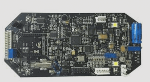
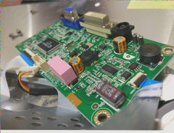
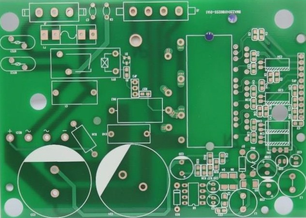
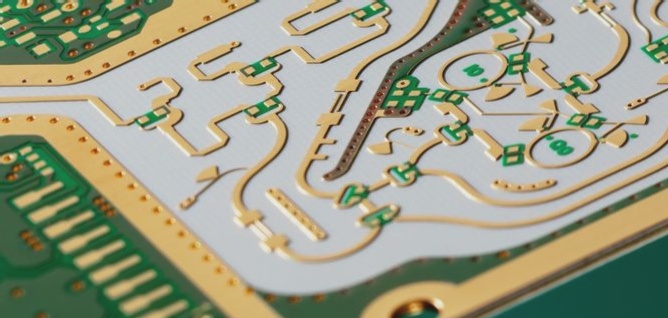
Various surface treatment processes, including Hot Air Solder Levelling (HASL), Organic Solder Protection (OSP), Electroless Nickel Gold Immersion (ENIG), Silver Immersion, and Tin Immersion, play a vital role in protecting PCB copper layers from oxidation and damage. Understanding these treatments is essential for optimizing ICT processes on lead-free PCBs.
HASL Process in PCB Manufacturing
- HASL is the primary leaded surface treatment method in the industry.
- Advantages of HASL include cost-effectiveness, solderability maintenance, and automatic solder coverage for test pads and vias.
- Lead-free HASL replacement processes are gaining popularity due to environmental concerns.
- Limitations of HASL include surface flatness issues and restrictions with fine pin pitch cases.
Organic Solder Protective Agent (OSP) for PCBs
- OSP creates a protective layer on copper surfaces to prevent oxidation during storage and assembly.
- Advantages of OSP include good coplanarity, lead-free process, and improved solderability.
- Disadvantages of OSP involve the need for significant process changes, potential damage during ICT testing, and reduced test repeatability.
Electroless Nickel Gold Immersion (ENIG) Coating
- ENIG provides a flat surface and excellent solderability but comes with a higher unit cost.
- Advantages of ENIG include good solderability, flat surface, and long shelf life.
- Disadvantages of ENIG consist of high cost, potential “black lumps” issue, and the use of harmful chemicals in the manufacturing process.
Silver Immersion
Additional information on silver immersion is currently being researched and will be updated soon.
Silver Immersion for PCB Boards
- Silver immersion is a surface preparation method for PCB boards.
- Mainly used in Asia, it is gaining popularity in North America and Europe.
- The silver layer melts into the solder joint during the soldering process, creating a reliable solder joint for BGA packages.
- Contrasting color for easy inspection.
- Natural alternative to HASL for soldering treatments.
- Advantages include good weldability and smooth surface.
- End users are conservative about this new technology.
Tin Immersion Process
- Newer surface treatment process similar to silver immersion.
- Health and safety concerns due to thiourea used in the process.
- Migration issues can be controlled with anti-migration chemistries.
- Advantages include good weldability and smooth surface.
- Concerns about health and safety and limited thermal cycling cycles.
Both silver immersion and tin immersion are promising surface treatment processes for PCB boards, each with its own set of advantages and challenges. Manufacturers are exploring these methods as potential lead-free alternatives for reliable solder joints.
Main Method of Lead-Free Processing of PCB Boards
Users have reported pass yields between 80-90% after addressing fixture and process issues. HASL remains a popular PCB processing method, especially in countries where alternatives to HASL have been banned by law. However, as PCB manufacturing expands into new areas, more lead-free processes like OSP are being explored as alternatives. While OSP may not be a direct replacement for HASL, it offers unique benefits such as force absorption, which is crucial for ICT testing.
Comparative Analysis of Surface Finishing Techniques
When comparing HASL, OSP, and Silver Immersion in the ICT phase, it’s important to consider how each technique impacts ICT performance. HASL, with its soft solder “arcs” and exposed vias, provides ideal test points for ICT. In contrast, OSP creates a hard “shell” on test targets, making direct probing challenging and potentially causing internal shorts.
Challenges and Recommendations for OSP in ICT Testing
- Delivery time to ICT should be less than 24 hours to avoid OSP-related issues.
- Factors like OSP provider type, reflow oven passes, and testing methods can affect OSP performance.
- Probing exposed copper surfaces on OSP boards can lead to copper layer breakage and shorts.
- Following “OSP Rules” for ICT test fixtures and procedures can help mitigate OSP-related challenges and ensure reliable test contact.
Considerations for Manufacturers
While some manufacturers see immediate cost savings from OSP as a lead-free alternative, others are re-evaluating their strategies due to production disruptions and delays associated with OSP. It’s essential for manufacturers to weigh the benefits and challenges of OSP carefully before adoption.
Silver Immersion
Content related to Silver Immersion processing is not available in the original text.
Silver Immersion: A Natural Alternative to HASL
- Silver immersion, a 0.4 to 0.8 micron metal layer on copper, provides a solid base for test probes.
- Initial research indicates it as a viable alternative to HASL in manufacturing processes.
- Surface roughness and thickness are key factors for ICT repeatability.
- Etch rate determines the shine of the silver finish in ICT testing.
Industry Insights
- ICT engineers should note the shift towards OSP as a HASL replacement for cost savings.
- OSP-coated PCBs may require solder-covered test pads for optimal performance.
- Consider all lead-free PCB processes to weigh advantages and disadvantages.
- Manufacturers now offer silver finish boards at competitive prices.
Future Prospects
- Research on silver immersion’s impact on ICT is limited but promising.
- No reported issues with gripper contact using silver finish in ICT.