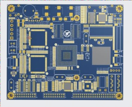
The Concept of Double-Sided PCB Board Prototype
A double-sided PCB board prototype consists of a substrate with two layers of copper foil circuits separated by insulating materials. This design allows for the creation of conductive holes, facilitating circuit connections on both sides of the board.

Benefits and Applications
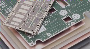
A double-sided PCB board prototype offers more wiring flexibility and is suitable for complex circuits. It is widely used in high-tech industries such as telecommunications, computers, medical equipment, and aerospace defense.
Comparison with Single-Sided PCB
- Single-sided PCB: Components on one side, wires on the other; difficult wiring.
- Double-sided PCB: Components and wiring on both sides; less wiring difficulty, suitable for complex circuits.
Production Process
The production process of double-sided boards involves cutting, drilling, copper deposition, etching, and more intricate steps compared to single panels.
Structural Similarities
Both single-sided and double-sided PCBs share common structures like solder pads, vias, mounting holes, connectors, and electronic components.
Working Levels of PCB Board Prototypes
- Signal Layer: Stores components related to signals
- Silk Screen Layer: Draws component appearance and prints product details
- Solder Mask Layer: Prevents solder flow and contamination
- Solder Paste Layer: Facilitates SMD component soldering
- Grounding Layer: Connects ground wire components
Benefits of Double-Sided PCB Board Prototypes
- Higher signal transmission rate
- More reliable circuit connection
- Larger usable area
- More convenient for wiring and debugging