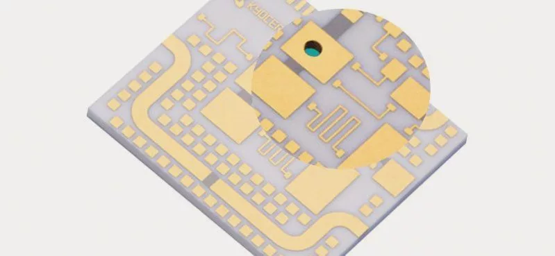
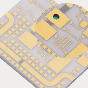

LTCC ceramic-based substrates are a 3-dimensional system of integration that integrates intricate digital and microwave circuits that utilize new ceramics and microwave thick-film integration technology. With the rapid advancement of monolithic integrated technologies, the integrated devices are increasing in frequency and reaching a new degree, making the integration of passive devices crucial. LTCC technology can satisfy the integration needs for passive devices, such as capacitors, resistor filters, couplers, and inductor.
Its resistance for LTCC substrate is 10O 100 O, 1K O, and 10K O. The accuracy of the surface resistance adjustment is less than 1% and the precision of internal embedded resistance is not more than 30 percent. Other passive devices are developed according to materials parameters. LTCC substrates can have multi-layer wiring with that is, up to 40 layers.
Low Temperature Co-fired Ceramic PCB (LTCC PCB )
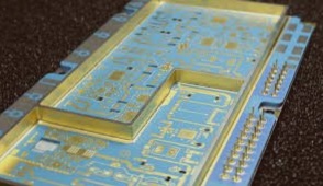
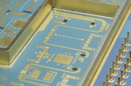
Recently, the Ceramic substrate technologies have evolved quickly, particularly in comparison to traditional ceramic substrate, high temperature co fired ceramic substrate as well as low temperature CO fired ceramic substrates are being developed. This allows the ceramic substrate to be used for high-density assemblies of high-power circuits gain a more extensive and more extensive applications. The low-temperature co fired multilayer substrate is an innovative micro assembly material that highlights the benefits of a thin film technology and co-firing at high temperatures. Over the past ten years, this type of substrate was developed quickly. Being a high density super-fast circuit board it’s extensively used for communication, computer rocket, missile and many other fields. As an example, Dupon company of the United States uses 8-layer low temperature multilayer co-fired substrate to test the circuit of the missile stinger. Fujitsu from Japan utilizes 61 layers of low temperature co-fired ceramic substrates to create the multi-chip module for the vp2000 series supercomputer. NEC company has created the 78-layers of co-fired low temperature multi-layer substrate that has an area that is 225 x 225 millimeters. It is equipped with 11540 I/O terminals and is able to install 100 VLSI chips.
Multilayers with low temperatures that co-fire ceramic substrate is composed from a number of ceramic substrates. Each substrate comprises the ceramic layer and electrical circuits connected on the surface of the ceramic typically referred to as the conduction band. The holes that run through the layer of ceramic are filled with conductors. They connect the conduction band lines of different layers of ceramic in a 3D circuit network. Its IC chip is positioned in the upper layer that is made of ceramics with multilayers. The block integrated is joined to the circuit within the ceramic multilayer substrate via pins that create the interconnection circuit. The conductive metal layer over the substrate is created ahead of time during the process of sintering the ceramic substrate. Additionally, there are needle-shaped terminals in the lower part of the surface. This way, the multilayer ceramic substrate is utilized to join the micro-components into a 3D structure that is high in density, with rapid speed, and high-reliability.
In comparison to other PCB-related technologies , LTCC PCB has numerous advantages
1. Ceramic materials possess excellent properties that include high frequency transmission at high speeds and a wide band. The dielectric constant in materials with LTCC is able to vary over the range of the components. Metal materials which have high conductivity for conductor materials could improve the efficiency of circuits and improve the design flexibility;
2. It is able to adapt to the demands of the high-current as well as high temperature resistance and is more thermally efficient over conventional PCB circuit boards. It significantly improves the cooling design of electronic devices, and has excellent reliability and is able to be utilized in extreme environments as well as extend the life of its use;
3. A circuit board that has multiple layers can be made with several passive components could be integrated into it to reduce the expense of packaging the components. In the 3-dimensional circuit board with a lot of layers, active and passive integration is possible that can assist in increasing the density of assembly in the circuit, and also reducing the weight and volume;
4. It’s compatible with different multi-layer wiring technology such as the use of LTCC in conjunction with thin-film wiring technology will result in more assembly density, and improve the efficiency of the hybrid multi-layer substrates and multi-chip modules;
5. This method of production makes it convenient for examination of the quality of every layer of wire and holes for interconnection before the final product is created that is helpful in increasing the quality and yield of the multilayer substrate while also shortening the time to produce and cutting the price.
6. Material saving, energy saving eco-friendly and sustainable have been a trend that is gaining momentum within the industry of components. LTCC can also meet the growing demand for this and helps reduce the impact on the environment caused by waste, raw materials as well as the production processes to the maximum extent.
Shape: max. 100 mm x 100 mm
Line width/space: min.0.075mm/0.15mm
Conductors printed with thickness of 10 – 25 mM
Line width precision: +/- 10mM
The accuracy of alignment for stacks:+ 30 m M
Diameter of hole through: min.0.1mm
Sintering shrinkage precision: +/- 0.2 percent
The distance between the conductor and the edge of shape: min.0.2mm
The distance between the hole and the line: min.0.15mm
Distance of overlap between resistance and Conductor min.0.15mm
Size of resistance: min.0.15mm x 0.15mm
The total number of layers in the media Total number of media layers: =40 layers
Application : Filter PCB, diplexer PCB, LTCC chip antenna PCB
If you have PCB technical issues, WellCircuits knowledgeable support team will be there to assist you through every step. It is also possible to ask for the PCB quotation via this link. You can contact us via email at info@wellcircuits.com
We’ll be in touch very fast.