8W Superconducting Aluminum Substrate PCB — WellCircuits
TL;DR
The 8W superconducting aluminum substrate PCB — more precisely described as an 8 W/(m·K) thermal conductivity insulated metal substrate (IMS) PCB — uses an aluminum base with a thermally conductive dielectric layer achieving 8 W/(m·K) thermal conductivity. This is approximately 3–4× higher than standard IMS dielectrics (1–3 W/m·K) and dramatically better than FR-4 (≈ 0.3 W/m·K). These boards excel in LED driver circuits, high-power LED array applications, automotive headlight thermal management, and power converter stages where 20–100 W/in² power density is required. WellCircuits manufactures 8 W/(m·K) IMS PCBs with aluminum bases from 1.5–3mm, dielectric thicknesses from 75–200μm, and copper circuitry from 35–105μm.
What Is an 8W/(m·K) Thermal Conductivity Aluminum Substrate PCB?
The term "8W superconducting aluminum substrate" refers to an insulated metal substrate (IMS) PCB where the dielectric layer achieves a thermal conductivity of 8 W/(m·K). This is a significant performance tier above standard IMS dielectrics, which typically range from 1–3 W/(m·K). The aluminum base provides bulk thermal spreading, while the high-performance dielectric enables efficient heat transfer from circuit components to the aluminum core.
The "8W" designation comes from the industry convention of quoting thermal conductivity in watts per meter-kelvin (W/m·K). A dielectric with 8 W/(m·K) thermal conductivity transfers heat roughly 3–4× more efficiently per unit thickness than a standard 2 W/(m·K) dielectric, enabling either higher power density per board area or thinner dielectric for the same thermal performance.
It is important to clarify the terminology: the aluminum substrate itself has a thermal conductivity of approximately 167 W/(m·K) for 6061 aluminum alloy. The dielectric layer — the electrically insulating layer between the copper circuitry and the aluminum base — is the performance bottleneck, and an 8 W/(m·K) dielectric represents the upper performance tier for polymer-based IMS dielectrics.
How 8 W/(m·K) IMS Compares to Alternatives
| Substrate Type | Thermal Conductivity | Relative Performance | Typical Application |
|---|---|---|---|
| Standard FR-4 | 0.3 W/m·K | 1× baseline | Consumer electronics |
| Standard IMS dielectric | 1–3 W/m·K | 3–10× FR-4 | LED lighting, industrial |
| 8 W/(m·K) IMS dielectric | 8 W/m·K | 25× FR-4 | High-power LED, automotive |
| Metal core PCB (aluminum) | N/A (base only) | N/A | Bulk heat spreading |
| DBC Alumina | 20–30 W/m·K (ceramic) | 65–100× FR-4 | IGBT, SiC power modules |
| Aluminum Nitride (AlN) | 150–180 W/m·K | 500–600× FR-4 | GaN, SiC high-power RF |
The 8 W/(m·K) IMS sits in the mid-range between standard IMS and ceramic substrates, offering a cost-effective solution for applications that need more thermal performance than standard IMS can provide but where the full thermal capability of DBC alumina is not required.
Manufacturing 8 W/(m·K) Aluminum Substrate PCBs
High-Thermal-Conductivity Dielectric Materials
The dielectric layer in an 8 W/(m·K) IMS PCB is typically a ceramic-filled polymer composite. The thermal conductivity improvement over standard IMS comes from loading the polymer matrix (typically polyimide, polyester, or epoxy) with a high-volume fraction of ceramic filler particles — commonly aluminum nitride (AlN), alumina (Al₂O₃), or boron nitride (BN).
The key to achieving 8 W/(m·K) is reaching a filler loading of approximately 60–70% by volume while maintaining electrical resistivity above 10¹² Ω·cm and dielectric breakdown strength above 20 kV/mm. These ceramic-filled dielectrics are available from specialty laminate suppliers such as Bergquist (now part of Henkel), The Bergquist Company, and Ventec International.
Common material grades achieving 8 W/(m·K) include:
- Bergquist HI-TMS series — polyimide-ceramic composite, Tg ≥ 200°C, 8 W/(m·K)
- Ventec VT-5B — epoxy-ceramic IMS material, 8 W/(m·K), UL 94 V-0
- Custom ceramic-filled epoxy systems — available from laminate specialists for volume applications
Lamination and Circuit Formation
The manufacturing process for 8 W/(m·K) IMS follows standard IMS fabrication:
1. Base preparation: The aluminum substrate (6061-T6 or 5052-H32) is cleaned, chemically treated (chromate or chrome-free conversion coating), and optionally pre-drilled for mounting holes.
2. Dielectric lamination: The ceramic-filled polymer dielectric prepreg is laminated to the aluminum base under heat (160–200°C) and pressure (200–400 psi), fully curing the polymer matrix.
3. Copper lamination: Circuit copper foil (typically 35μm for standard circuits, 70μm for power buses) is laminated onto the dielectric layer.
4. Circuit patterning: Standard photolithography and etching forms the copper circuit traces.
5. Surface finish: ENIG, HASL, or OSP is applied to exposed copper surfaces.
6. Solder mask: Epoxy solder mask is applied and cured, typically white for LED applications.
7. Electrical test: 100% continuity and isolation testing verifies all circuits.
The key process control difference from standard IMS is the lamination temperature and pressure profile, which must fully consolidate the ceramic-filled composite without void formation. Voids in the dielectric create thermal hot-spots and reduce effective thermal conductivity by up to 30%.
Thermal Resistance Calculation
For an 8 W/(m·K) dielectric of thickness d (in meters), the thermal resistance from the component to the aluminum base is:
Rth = d / (k × A)
Where:
- d = dielectric thickness (m)
- k = 8 W/(m·K)
- A = contact area between component and dielectric (m²)
For a 10mm × 10mm QFN package on a 100μm (0.0001m) dielectric:
- Rth = 0.0001 / (8 × 0.0001) = 0.125°C/W
This compares to approximately 0.33°C/W for a standard 2 W/(m·K) dielectric at the same thickness — a 2.6× improvement.
Real-World Applications
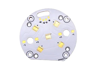
1. High-Power LED Driver Circuits
LED driver ICs and MOSFET power stages in high-brightness LED luminaires (100–500 W) generate 10–50 W of heat that must be removed to maintain driver IC junction temperatures below 125°C. An 8 W/(m·K) IMS substrate under the driver stage enables a 75μm dielectric that provides both thermal performance (Rth ≈ 0.1°C/W per cm²) and adequate electrical isolation (typically 1.5–3 kV).
In a typical 200W LED streetlight driver, the AC-DC PFC stage and DC-DC LED driver are co-located on a single 8 W/(m·K) IMS board mounted directly to the luminaire housing, eliminating the need for a separate heat sink.
2. Automotive Headlight LED Array Thermal Management
Automotive LED headlights for premium and mid-market vehicles operate at 30–100 W per headlight assembly using multi-chip LED arrays. The thermal path from the LED die to the headlight housing must manage 30–100 W while maintaining the LED junction at < 130°C for rated lifetime.
An 8 W/(m·K) IMS board with 75μm dielectric under each LED cluster provides a junction-to-housing thermal resistance of approximately 0.1°C/W per cm² of LED footprint. For a 50W LED array occupying 20cm², the temperature rise from junction to housing is approximately 2.5°C — well within acceptable limits when the housing temperature is maintained at < 90°C by the vehicle's thermal management system.
3. Battery Management System (BMS) Power Stage
EV and hybrid vehicle battery management systems handle 5–30 kW of continuous power throughput, with MOSFET/IGBT switching stages generating 50–200 W of heat per module. The 8 W/(m·K) IMS substrate allows the BMS power stage to be mounted directly to the vehicle chassis or battery pack enclosure, using the metal structure as a heat sink without requiring electrical isolation另行.
This direct chassis mounting eliminates the weight and cost of a separate isolated heat sink, reducing the BMS module weight by 15–30% compared to designs using standard FR-4 with separate insulator and heat sink.
4. Motor Drive Power Module Output Stage
Three-phase BLDC or PMSM motor drives for industrial automation, robotics, and e-bikes use high-frequency MOSFET bridges that switch at 15–30 kHz. The 8 W/(m·K) IMS substrate under the three half-bridge switching stages handles the combined switching and conduction losses while maintaining the MOSFET junction temperature below 150°C.
The ability to mount the motor drive PCB directly to an aluminum mounting plate or motor housing — using the motor's thermal mass as a heat sink — is a key advantage in space-constrained applications like collaborative robot joints (cobots) where every cubic centimeter is critical.
5. RF Power Amplifier Final Stage
S-band and C-band RF power amplifiers for wireless infrastructure (4G/5G base stations) and industrial heating (RF plasma generation) use LDMOS or GaN-on-SiC transistors in the final stage. These devices dissipate 50–300 W of heat that must be transferred to the chassis heat sink with minimal thermal resistance.
The 8 W/(m·K) IMS substrate, with its combination of high thermal conductivity and controlled dielectric constant (typically 3.5–5.0), provides a single material solution for both the thermal path and the RF substrate requirements, simplifying the power amplifier module assembly.
Design Considerations
1. Dielectric Thickness Selection for Thermal vs. Isolation Trade-Off
The primary design decision for 8 W/(m·K) IMS is choosing the dielectric thickness that balances thermal performance against voltage isolation:
| Dielectric Thickness | Thermal Resistance (per cm²) | Isolation Voltage | Typical Use |
|---|---|---|---|
| 50μm | 0.063°C/W | ~1 kV AC | GaN power stages, high-power LEDs |
| 75μm | 0.094°C/W | ~1.5 kV AC | Automotive LED drivers, BMS |
| 100μm | 0.125°C/W | ~2 kV AC | Industrial motor drives |
| 150μm | 0.188°C/W | ~3 kV AC | High-voltage EV applications |
| 200μm | 0.25°C/W | ~4 kV AC | Isolation voltage priority |
The 8 W/(m·K) dielectric achieves approximately 2.5–4× better thermal resistance than a standard 2–3 W/(m·K) IMS at the same dielectric thickness.
2. Thermal Via Enhancement for High-Power Components
For components mounted with thermal vias directly over the aluminum base (where the dielectric has a thermal via land pattern), thermal via arrays provide a supplementary heat path. A typical thermal via array under a power MOSFET uses:
- Via diameter: 0.3–0.5mm (larger than standard PCB thermal vias due to dielectric processing constraints)
- Via pitch: 0.6–1.0mm (center-to-center)
- Via fill: Non-plated (open) thermal vias filled with thermal epoxy or left open for forced-air cooling; or copper-plated thermal vias for maximum heat transfer
Plated thermal vias in IMS boards can achieve effective thermal conductivities of 20–40 W/(m·K) when the via barrel is filled with copper, providing a 2.5–5× improvement over the dielectric alone.
3. Copper Weight Selection for Power Density
The copper trace weight on 8 W/(m·K) IMS is selected based on current carrying requirements and thermal contribution:
- 35μm (1 oz/ft²) — Standard signal traces and low-power circuits
- 70μm (2 oz/ft²) — Power distribution traces, MOSFET drain/Source planes
- 105μm (3 oz/ft²) — High-current bus bars (up to 30 A per mm width), LED arrays
Heavier copper contributes to thermal spreading in two ways: it distributes current-related I²R heat across a wider area before it enters the dielectric, and the copper's own thermal conductivity (387 W/m·K) provides lateral heat spreading.
4. CTE Mismatch and Thermal Cycling Reliability
The coefficient of thermal expansion (CTE) of the 8 W/(m·K) ceramic-filled dielectric is approximately 20–35 ppm/°C, which falls between the copper traces (17 ppm/°C) and the aluminum base (23 ppm/°C). This relatively good CTE match reduces delamination risk during thermal cycling compared to standard epoxy IMS dielectrics (CTE ≈ 50–70 ppm/°C).
However, the ceramic filler loading makes the dielectric more rigid and less compliant. Recommendations for high-reliability applications:
- Clip-mounting rather than rigid bolting for board mounting
- Underfill for BGA and QFN packages above 5W
- Corner stress relief features in the dielectric layout
- Thermal cycling qualification per IPC-6012 Class 3 (−40°C to +125°C, minimum 500 cycles)
Compliance and Standards
8 W/(m·K) aluminum substrate PCBs are evaluated against these standards:
- IPC-6012 Class 3 — Applies to the board-level quality and reliability requirements, including dielectric adhesion, conductor integrity, and thermal cycling acceptance.
- IPC-A-600 — Visual acceptance criteria for the finished substrate, with specific provisions for IMS dielectric appearance (no voids, cracks, or delamination).
- UL 94 V-0 — Flammability rating. All standard 8 W/(m·K) IMS dielectrics are rated V-0. The aluminum base is inherently non-combustible.
- RoHS 2 / RoHS 3 (2011/65/EU) — Restriction of hazardous substances. Standard ceramic-filled IMS dielectrics and 6061/5052 aluminum alloys are RoHS compliant. Lead-free surface finishes are standard.
- REACH (EC 1907/2006) — Chemical registration and restriction. All WellCircuits IMS materials are REACH compliant with full REACH declarations available.
- AEC-Q101 — Stress qualification for discrete semiconductor devices assembled on 8 W/(m·K) IMS substrates, required for automotive LED and BMS applications.
- IATF 16949 — Automotive quality management system. WellCircuits maintains IATF 16949 certification for automotive IMS substrate production.
FAQs
What does "8W" mean in aluminum substrate PCB specifications?
The "8W" refers to the thermal conductivity of the dielectric layer, stated as 8 W/(m·K). This means that for every meter of dielectric thickness, 8 watts of heat will flow per kelvin of temperature difference. In practical terms, a 100μm (0.0001m) dielectric transfers 8 / 0.0001 = 80,000 W/m² per °C — approximately 3–4× better than standard IMS dielectrics.
What is the thermal resistance of an 8 W/(m·K) IMS PCB?
For a 75μm dielectric, the thermal resistance is approximately 0.094°C/W per cm² of component footprint. A 10mm × 10mm (1 cm²) power device on 75μm 8 W/(m·K) dielectric generates a temperature rise of approximately 9.4°C at 100W power dissipation.
How does 8 W/(m·K) IMS compare to DBC alumina for LED headlight thermal management?
DBC alumina (20–30 W/(m·K) ceramic) handles higher power densities (>200 W/in²) and operates at higher junction temperatures (GaN/SiC up to 200°C). However, 8 W/(m·K) IMS is 5–10× less expensive, easier to manufacture in complex shapes, and the aluminum base provides superior thermal spreading for the typical 50–150 W headlight application.
What aluminum thickness is used for 8 W/(m·K) IMS substrates?
Standard aluminum thicknesses range from 1.0–3.0mm. Thicker aluminum (2–3mm) provides better thermal spreading and structural rigidity for large panels. Thinner aluminum (1.0–1.5mm) is used for weight-critical applications and cost reduction where thermal spreading is less critical.
What surface finishes are available for 8 W/(m·K) IMS PCBs?
Standard finishes include HASL-LF (lead-free hot air solder leveling), ENIG (electroless nickel immersion gold), OSP (organic solderability preservative), and hard gold (25–50μm nickel/gold) for connector contacts. White solder mask is standard for LED applications due to its high reflectivity (>80% at 450nm).
Is 8 W/(m·K) IMS suitable for automotive applications?
Yes. 8 W/(m·K) IMS with AEC-Q101-qualified components is used in automotive LED headlights, BMS power stages, and motor drives for EV applications. The IATF 16949-compliant production at WellCircuits ensures traceability and process control required for automotive qualification.
Get Your 8 W/(m·K) IMS PCB Made at WellCircuits
WellCircuits manufactures high-thermal-conductivity insulated metal substrate PCBs using ceramic-filled dielectric systems rated at 8 W/(m·K). Our IMS production line supports panel sizes up to 500mm × 600mm, custom step-dielectric profiles, thermal via arrays, and full electrical test including hi-pot testing up to 5 kV DC.
Capabilities at a glance:
- Dielectric thermal conductivity: 8 W/(m·K) (ceramic-filled polymer composite)
- Aluminum base: 1.0–3.0mm (6061-T6, 5052-H32)
- Dielectric thickness: 50–200μm (optimized per application)
- Copper weight: 35–105μm (1–3 oz/ft²)
- Max panel size: 500mm × 600mm
- Thermal resistance: 0.06–0.25°C/W per cm² (per dielectric zone)
- Surface finish: ENIG, HASL-LF, OSP, hard gold
- Solder mask: white (LED), black, clear
- Standards: IPC-6012 Class 3, AEC-Q101, IATF 16949, RoHS 3
Upload your Gerber files, thermal budget data, and dielectric thickness requirements to receive a manufacturing feasibility review and production quote within 24 hours.
[Get a Quote →](https://wellcircuits.com/quote/) [IMS PCB Capabilities →](https://wellcircuits.com/ims-pcb/) [Contact Sales →](https://wellcircuits.com/contact/)