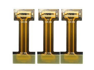
2-layer FLEX PCB
2-Layer FPC (Flexible Printed Circuit) — A Complete Design & Manufacturing Guide
A 2-layer flexible printed circuit (FPC) is a dynamic-flex interconnection solution built on polyimide substrate with two conductive layers. Adhesiveless construction eliminates flow contamination risks. Coverlay dielectrics protect traces while maintaining bend radii down to 3× material thickness. These boards serve high-volume consumer electronics where repeated flexing demands reliability over thousands of cycles.
What Is a 2-Layer FPC?
A 2-layer FPC consists of two copper conductor layers separated by a polyimide dielectric core, with polyimide coverlays laminated over the outer surfaces. Unlike rigid PCBs, FPCs are designed to bend during installation (static flex) or during operation (dynamic flex). The term "adhesiveless" refers to constructions where the copper is cast directly onto the polyimide film rather than bonded with acrylic or epoxy adhesive — a distinction that matters significantly for high-reliability applications.
The base material for most production-grade 2-layer FPCs is DuPont Pyralux series films, specifically Pyralux LF (adhesiveless copper-clad laminate) rated for continuous service temperatures from -40°C to +130°C. Alternative substrates include Kapton HN and AP films from DuPont, and equivalent polyimide films from Kaneka and UBE Industries.
The two copper layers are typically 12μm (0.5 oz) or 18μm (0.75 oz) electrodeposited (ED) copper, though rolled-annealed (RA) copper is specified for dynamic flex applications where crack resistance at bend points is critical. A 12μm polyimide film serves as the core dielectric, with dielectric withstand voltage typically rated at 1.5–2 kV AC per IPC-6012 Class 2 requirements.
Manufacturing Process for 2-Layer Adhesiveless FPC
Step 1 — Base Material Preparation
The process begins with adhesiveless copper-clad laminate (CCL), where rolled-annealed copper is applied to polyimide film through a vapor deposition orcasting process. For dynamic flex applications, many manufacturers specify RA copper with a 20μm minimum thickness in the bend zone to resist crack propagation. The CCL is inspected per IPC-A-600 for surface defects, voids, and dimensional compliance before entering production.
Step 2 — Circuit Patterning
Photoresist is applied to the copper surface, exposed to UV light through a film artwork or direct laser imaging (LDI) system, and developed to reveal the circuit pattern. The exposed copper is then etched using alkaline ammoniacal or acidic cupric chloride etchants. Etch factor — the ratio of depth to width undercut — should exceed 3:1 for fine-line applications (≤100μm line width) to maintain trace sidewall verticality.
Step 3 — Via Formation and Metallization
Plated through-holes (PTH) connect the two copper layers. For 2-layer FPCs, this is typically accomplished via mechanical drilling or laser drilling (CO2 or UV laser), followed by desmear treatment and electroless copper deposition to establish interlayer connectivity. Via barrel copper thickness is specified per IPC-6012 Class 2 or Class 3 depending on end application — typically 20–25μm minimum for Class 2, 25μm minimum for Class 3.
Step 4 — Coverlay Lamination
Liquid photoimageable (LPI) soldermask or polyimide coverlay film is applied over the outer circuit layers. Coverlay film (typically 25μm or 50μm polyimide with acrylic or thermoset adhesive) is laminated at elevated temperature and pressure. PTH openings are punched or laser-ablated through the coverlay. For high-temperature applications (>150°C operating temperature), thermoset adhesive-free coverlay is preferred to eliminate acrylic flow risk.
Step 5 — Surface Finish and Final Processing
The board receives a surface finish appropriate for the assembly method: ENIG (electroless nickel immersion gold, ~3–5μm nickel over ~0.05μm gold) for soldering; OSP (organic solderability preservative) for low-temperature assembly; or bare copper with ENEPIG for gold-wire bonding. The panels are routed or laser-cut to final shape, inspected per IPC-A-600, and packed with tension-relief folding instructions.
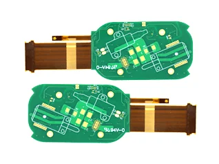
Real-World Applications
1. Smartphone Display Interconnects
FPCs carry signals between display modules and main processor boards in smartphones. A typical flagship smartphone contains 3–5 FPC assemblies totaling 40–60cm of flexible circuitry, with 2-layer constructions handling data bus, power, and touch sensor connections. Display FPCs typically specify 50μm line/space resolution with impedance-controlled differential pairs for MIPI DSI interfaces.
2. Wearable Device Sensor Connections
Smartwatches and fitness trackers demand miniaturized interconnects that flex during wrist movement. A 2-layer FPC for wearable applications typically uses 12μm copper on 25μm polyimide substrate to minimize thickness (total stackup often ≤100μm). Dynamic flex life requirements range from 10,000 to 50,000 cycles at bend radius of 0.5–1.0mm per IEC 60335-1 bend testing protocols.
3. Automotive Instrument Cluster Harnesses
Modern automotive instrument clusters use FPCs to replace heavy ribbon cable assemblies, reducing weight and simplifying assembly. Automotive FPCs must pass AEC-Q100 temperature cycling (-40°C to +85°C operating, -40°C to +105°C storage) and vibration testing per MIL-STD-883 Method 2007. The 2-layer construction provides sufficient routing density for LED backlight and display driver connections.
4. Medical Device Internal Cabling
Endoscopic cameras, patient monitors, and portable diagnostic equipment use 2-layer FPCs for their combination of flexibility and sterility compatibility. Medical FPCs typically require IPC-6012 Class 3 qualification with 100% electrical continuity testing and visual inspection per IPC-A-610 acceptability criteria. Biocompatibility per ISO 10993 may be required for devices with patient contact.
5. Notebook Computer Hinge Assemblies
The cable assemblies routing signals through notebook hinges must survive 20,000–50,000 open-close cycles without signal degradation. 2-layer FPCs with reinforced strain-relief sections (locally thickened with additional polyimide layers) handle this application. Folded or rolled-stiffener construction near the hinge axis provides crack resistance where copper traces cross the bend axis at a 90° angle.
6. Drone and UAV Control Linkages
Lightweight, high-reliability interconnects for drone flight controllers and gimbal stabilization systems use 2-layer FPCs to minimize weight while providing impedance-controlled signal routing. Typical stackup for UAV FPCs: 18μm RA copper / 25μm polyimide / 18μm RA copper, with overall thickness of 70–80μm before stiffener addition.
Design Considerations for 2-Layer FPC
Tip 1 — Specify RA Copper for Dynamic Flex Zones
Electrodeposited (ED) copper has a grain structure oriented perpendicular to the plane of the foil, which creates stress concentration at grain boundaries during repeated bending. Rolled-annealed (RA) copper has elongated grain structure parallel to the surface, providing superior crack resistance in bend zones. Specify RA copper for any area that will flex more than 100 times during product life. For applications exceeding 100,000 cycles, consider high-elongation RA copper (35%+ elongation at break per ASTM E345).
Tip 2 — Avoid 90° Trace Angles at Bend Zones
Route traces at ±45° angles when approaching a bend zone rather than routing at 90° to the bend axis. Sharp corners in copper traces create mechanical stress concentration that accelerates crack initiation. The preferred practice is a mitered (45°) or curved routing approach with a minimum bend radius of 3× total stackup thickness. For a 100μm total stackup, minimum bend radius = 300μm.
Tip 3 — Reinforce Termination Areas
Any area where the FPC connects to a connector, stiffener, or rigid PCB requires reinforcement. Stiffener materials include polyimide (same as substrate), FR4, or stainless steel shim. Stiffener thickness typically ranges from 0.1mm to 0.3mm depending on mechanical load. Extend stiffeners at least 2mm beyond the interface edge to prevent adhesive peel at the termination.
Tip 4 — Account for Dimensional Tolerance Stack-Up
FPCs have wider dimensional tolerances than rigid boards due to polyimide's thermal expansion coefficient (~20 ppm/°C vs ~6–8 ppm/°C for FR4) and the stretch characteristics of the base film. Allow ±0.3mm tolerance on overall panel dimensions and ±0.15mm on feature-to-edge distances. For high-density connector interfaces, specify custom artwork scaling based on measured panel shrinkage rather than nominal dimensions.
Tip 5 — Validate Coverlay Opening Size for Soldering
Coverlay openings must provide adequate clearance for the component or connector pad while maintaining sufficient dielectric margin. IPC-6012 specifies minimum 100μm annular ring around PTH barrels and minimum 150μm spacing between coverlay opening edge and adjacent copper feature for Class 2 boards. For hand-soldered terminations, larger openings (≥ pad width + 300μm per side) reduce bridging risk.
Compliance and Testing Standards
2-layer FPCs are qualified to IPC-6012, the specification for rigid printed boards, with the Flexible Circuits Handbook (IPC-2223) serving as the primary design and qualification standard for flexible circuits. Key test methods include:
- IPC-6012 Class 2: General electronics — minimum insulation resistance of 500MΩ after humidity exposure, minimum conductor bond strength of 4N/cm
- IPC-6012 Class 3: High-reliability electronics — minimum insulation resistance of 1,000MΩ, minimum conductor bond strength of 5.5N/cm, 100% thermal stress testing
- IPC-A-600: Acceptability criteria for printed boards — defines surface finish acceptability, etch quality, and dielectric integrity thresholds
- IPC-2223 Section 4: Dynamic flex test methods — specifies bend radius, cycle count, and pass/fail criteria for dynamic applications
- UL 94: Flammability rating — most FPC base materials achieve VTM-0 or V-0 rating; required for consumer electronics
For automotive applications, additional qualification per AEC-Q100 (component-level) or AEC-Q200 (passive component-level) may apply, along with production part approval process (PPAP) documentation. Medical applications require ISO 13485 quality management system registration and IPC-6012 Class 3 certification with design history file (DHF) traceability.
Frequently Asked Questions
What is the difference between adhesiveless and adhesive-based 2-layer FPC?
Adhesiveless FPC uses copper that is cast or deposited directly onto polyimide film without intermediate adhesive layer. This eliminates adhesive flow risk during thermal processing and provides better Z-axis expansion characteristics. Adhesive-based constructions use acrylic or epoxy adhesive between polyimide layers and are typically lower cost but have reduced thermal stability (max 105°C operating vs 130°C for adhesiveless) and higher z-axis expansion coefficient.
What minimum bend radius can a 2-layer FPC achieve?
The minimum achievable bend radius for 2-layer FPC is typically 3× the total stackup thickness. For a standard construction (12μm copper + 25μm polyimide + 12μm copper = 49μm total), minimum bend radius ≈ 150μm. Dynamic flex applications should specify larger bend radii (6–10× stackup) to achieve acceptable cycle life. RA copper enables tighter radii than ED copper.
How does 2-layer FPC compare to 4-layer FPC for smartphone applications?
2-layer FPC is used for simpler signal routing where interconnect density requirements fit within two routing layers. 4-layer FPC adds two additional copper layers for higher routing density, impedance control, and shielding, but at higher material cost and reduced flexibility. Most smartphone display interconnects use 2-layer FPC; baseband and application processor interconnects more commonly use 4-layer or 6-layer rigid-flex constructions.
What surface finish is recommended for 2-layer FPC assembly?
ENIG (electroless nickel immersion gold) is the most common surface finish for FPC assembly because it provides flat topography, excellent solderability shelf life (12+ months), and compatibility with multiple reflow cycles. OSP is a lower-cost alternative suitable for single-reflow assemblies with shorter shelf life (3–6 months). For gold wire bonding, specify hard gold (electrolytic, ≥ 25μm) on pad areas or ENEPIG as a universal finish.
What is the typical thermal resistance of 2-layer FPC?
Polyimide has a glass transition temperature (Tg) of 250–260°C and continuous operating temperature rating of 200–250°C depending on specific grade. Thermal conductivity of polyimide film is approximately 0.12–0.20 W/m·K. For applications involving thermal dissipation, thermal vias (laser-drilled, filled with thermally conductive paste or solder) can be incorporated into the FPC design to provide heat transfer paths.
How is FPC thickness controlled for wearable applications?
Wearable FPCs minimize total thickness by specifying 12μm copper (0.5 oz) instead of standard 18μm (0.75 oz), using 25μm polyimide instead of 50μm, and avoiding stiffener in flexible zones. Total stackup for thin wearable FPC can reach 60–80μm compared to 150–200μm for standard constructions. Thickness tolerance is typically ±10% of total stackup, requiring careful control of lamination pressure and adhesive coverage.
What inspection methods verify 2-layer FPC quality?
Visual inspection per IPC-A-610 checks for coverlay delamination, conductor defects, and termination quality. Automated optical inspection (AOI) detects opens, shorts, and registration errors at line speeds suitable for production volumes. For buried features, X-ray inspection verifies PTH barrel fill and alignment. Electrical test (flying probe or bed-of-nails) confirms 100% continuity and insulation resistance before shipment.
Bottom Line
2-layer adhesiveless FPC is a mature, high-volume interconnection technology that balances flexibility, reliability, and cost for consumer electronics, automotive, and medical applications. The key decisions — adhesiveless vs adhesive-based construction, ED vs RA copper, ENIG vs OSP surface finish — cascade from your application requirements: dynamic vs static flex, operating temperature range, and assembly method compatibility.
For most smartphone and wearable applications, a 2-layer adhesiveless construction using Pyralux LF with ENIG finish and RA copper in bend zones provides the right combination of flexibility, thermal stability, and assembly compatibility. Automotive and medical applications require Class 3 qualification per IPC-6012 with full traceability documentation.
WellCircuits manufactures 2-layer FPC to IPC-6012 Class 2 and Class 3 specifications from our Shenzhen facility, with standard lead times of 10–15 working days for prototype quantities and volume production runs. Our engineering team reviews every FPC design for DFM compatibility before production. Request a quote or upload your design files to get started.
Need a Quote?
Fill in your requirements and get a detailed quotation within 24 hours.
Request a QuoteNo account required • Free consultation
Request a Quote
Fill in your requirements and we'll get back to you within 24 hours.