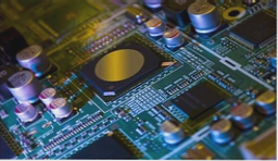
Key Considerations for Post-Layout PCB Design Inspection
After completing the layout and routing of a PCB, it is crucial to conduct a thorough post-layout inspection to ensure the board’s functionality and reliability.
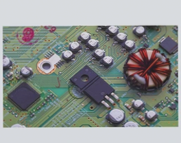
Component Packaging
During inspection, pay close attention to the following:
- Check the **Pad Pitch**: Ensure correct pad spacing for smooth soldering.
- Verify **Via Size** (if applicable): Adequate margin for through-hole components is essential for reliability.
- Inspect **Contour Silk Screen**: The silk screen outline should slightly exceed the component size for proper installation.
PCB Layout
Consider the following aspects of PCB layout:
- Proper **IC Placement**: Avoid placing ICs near the PCB edges.
- Effective **Component Grouping**: Group components logically based on circuit modules for optimal functionality.
- Strategic **Socket Placement**: Position sockets for easy installation and connection to other modules.
- Correct **Socket Orientation**: Ensure sockets are oriented correctly to avoid rewiring.
- Respect **Keep Out Areas**: Do not place components within designated “Keep Out” zones.
- Prevent **Interference**: Keep interference sources away from sensitive circuits to avoid signal disruption.
Wiring
Consider the following wiring guidelines:
- Optimal **Trace Width**: Choose appropriate trace width based on manufacturing process and current requirements.
- Maintain **Differential Signal Traces**: Ensure equal length, parallel running, and proper spacing for differential pairs.
- Handle **High-Speed Trace Return Path**: Keep trace and return path close to mitigate electromagnetic interference.
- Separate **Analog Signal Traces**: Keep analog traces away from interference sources and minimize their length.
EMC and Signal Integrity
Ensure signal integrity with the following practices:
- Include **Termination Resistors**: Add termination resistors for high-speed or long digital signal traces to prevent reflections.
- Implement **Input Signal Filtering**: Filter input signals to maintain signal integrity.
By meticulously inspecting these key elements, you can enhance the performance and reliability of your PCB designs.
Signal Integrity Tips for PCB Design
- Input signal lines from interfaces should be paired with a small capacitor (in the picofarad range) close to the input pin. The capacitor value should be selected based on the signal’s frequency and strength, ensuring it is not too large to avoid degrading signal integrity. For low-speed signals like key inputs, a 330pF capacitor is typical.
Driving Capability
- For signals with larger current requirements (such as switching signals), consider using a transistor to drive them. For buses with high fan-out, a buffer (e.g., 74LS224) can be added to ensure proper signal driving.
Silk Screen Guidelines
- Board Information: Include the board name, date, and part number (PN code) on the silk screen layer.
- Labeling Pins or Key Signals: Mark key pins or signals on interfaces clearly, especially for arrays or multi-pin connectors.
- Component Labeling: Place component labels in an easily readable and accessible location, avoiding crowded areas. Ensure labels do not overlap vias or obstruct other important features.
Additional Recommendations
- Mark Points: For PCBs requiring machine soldering, add two or three mark points to facilitate proper alignment and assembly.
If you have any questions about PCB design, please feel free to contact us at info@wellcircuits.com.