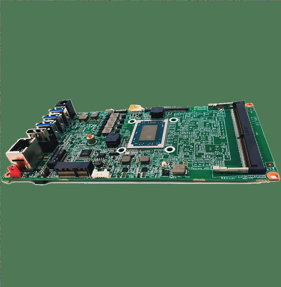
Power Line Layout in PCB Design
Power Cord Layout:
- Adjust the width of power traces based on current requirements, maximizing it whenever possible.
- Orient power and ground traces in alignment with the data flow direction.
- Include a 10~100μF decoupling capacitor at the PCB’s power input, opting for a value greater than 100μF if feasible.
Grounding Layout:
- Segregate digital ground from analog ground.
- Ensure ground traces are thick enough to handle at least three times the maximum current, typically 2~3mm wide.
- Create a continuous loop for the ground traces in the layout to minimize potential differences.
Decoupling Capacitor Configuration:
- Position a 10~100μF electrolytic capacitor across the PCB’s power input, opting for a higher value if possible.
- Utilize a 0.01~0.1μF ceramic capacitor between Vcc and GND for each integrated circuit.
- Include decoupling capacitors for components sensitive to noise, such as ROM and RAM.
Device Configuration:
- Place clock input pins of the clock generator, crystal oscillator, and CPU close together and away from low-frequency components.
- Keep low-current and high-current circuits separate from logic circuits.
- Position high-heat generating devices at the top of the PCB within the chassis for improved heat dissipation.
Separation of Power Lines, AC Lines, and Signal Lines:
Power and AC lines should be routed separately from signal traces on different layers or sections of the PCB to reduce interference.
Additional Layout Principles:
- Add a 10kΩ pull-up resistor to the bus for enhanced noise immunity.
- Ensure address lines are short and direct during routing.
- Arrange traces vertically on the PCB to minimize mutual interference.
- Size decoupling capacitors based on the data transmission frequency.
Use of Decoupling Capacitors
Consider utilizing decoupling capacitors strategically in your PCB design for optimal performance.
The Importance of Decoupling Capacitors in PCB Design
The decoupling capacitor plays a crucial role in integrated circuits by serving as an energy storage component and filtering out high-frequency noise. In digital circuits, a 0.1μF capacitor with 5μH inductance effectively decouples noise below 10MHz but has minimal impact on noise above 40MHz.
For better high-frequency noise filtering, capacitors with values of 1μF and 10μF, with higher parallel resonance frequencies above 20MHz, are recommended. It is advised to include an additional 10μF charge/discharge capacitor for every 10 integrated circuits, opting for tantalum or polycarbonate capacitors over electrolytic ones.
When selecting decoupling capacitors, a practical approach is to follow the formula C=1/F, using 0.1μF for 10MHz noise and 0.01μF for 100MHz noise. Short leads are essential when soldering capacitors to prevent self-resonance, as longer leads can affect the capacitor’s performance.
Eight Tips for Reducing Noise and Electromagnetic Interference in PCBs
- Use series resistors to reduce edge transition rates in the control circuit.
- Keep clock signal areas close to ground with short traces and encircle them with ground traces.
- Ground the positive input of unused operational amplifiers and connect the negative input to the output terminal.
- Avoid leaving unused gate circuit outputs floating.
- Use 45° bends for traces instead of 90° bends to reduce external radiation and signal coupling.
- Run clock lines perpendicular to I/O lines to minimize interference.
- Keep component leads short to minimize inductive effects.
- Avoid routing traces beneath sensitive components like quartz crystals.
PCB Manufacturing Circuit Distribution
In PCB manufacturing, the distributed capacitance introduced by packaging materials ranges from 2pF to 10pF. Connectors on circuit boards typically have a distributed inductance of 5 to 20μH, while a 24-pin dual-in-line integrated circuit socket adds a distributed inductance ranging from 4μH to 18μH, outlining the common circuit distribution in PCB manufacturing.