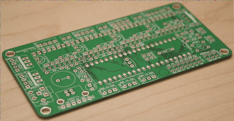
Wave Soldering PCB Circuit Boards Without a Carrier
Have you ever wondered when a PCB circuit board can undergo wave soldering without the need for a carrier or template? Let’s delve into this topic.
Historical Perspective
In the early days of PCBA assembly, carriers were rarely used. Most PCBs were directly subjected to wave soldering, except for cases where the board couldn’t support significant weight, like power boards.
Evolution of Wave Soldering
With the advent of selective wave soldering and the trend towards thinner, smaller PCB designs, the reliance on carrier systems has increased. This has led to scenarios where not all wave soldering processes necessitate a furnace carrier.
Essential Requirements for Wave Soldering Without a Carrier
- PCB Design Requirements:
- Reserve at least 5mm of the PCB’s edge for the wave soldering chain and PCBA placement.
- Ensure a PCB thickness of 1.6mm or more to prevent warpage and overflow.
- Maintain a gap of over 1.0mm between solder pads to prevent short-circuiting.
- Parts and Layout Requirements:
- Ensure SMD components are oriented perpendicularly to the board’s travel direction.
- Only accommodate certain components on the wave soldering area.
- Design through-hole components on the primary side with the correct orientation.
- Process Requirements:
- Secure SMD components with red glue on the wave soldering surface.
- Avoid including solder pads that cannot be wetted with solder on the wave solder contact surface.
- Cover non-wettable solder pads with high-temperature tape on the soldering furnace contact surface.
- Use short-foot operations for through-hole components to prevent short-circuiting.
Conclusion
By meeting these requirements, a PCB can successfully undergo wave soldering without the need for a carrier. Understanding these conditions is crucial for efficient PCB assembly processes.