Vias in PCB Boards: A Comprehensive Guide
Vias play a critical role in multi-layer PCB boards, with drilling costs typically making up a significant portion of production expenses. Essentially, any hole on a PCB can be considered a via.
Types and Functions of Vias:
- Electrical connection between layers
- Fixing or positioning devices
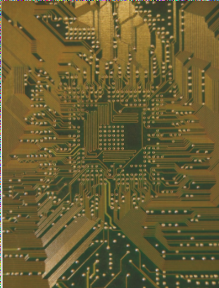
From a process standpoint, vias are commonly classified as blind vias, buried vias, and through vias:
- Blind vias are located on the top and bottom surfaces of the PCB, connecting surface and inner circuits.
- Buried vias are internal connection holes within PCB layers that do not extend to the surface.
- Through-holes penetrate the entire PCB and can serve as internal connections or component mounting locations.
Design Considerations:
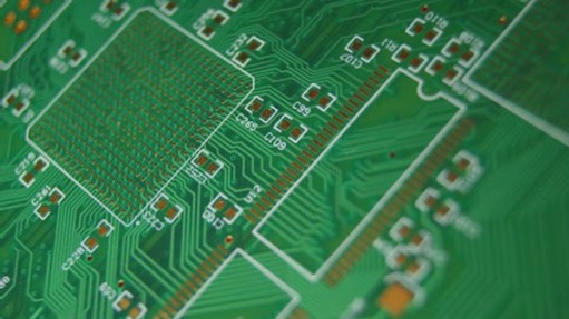
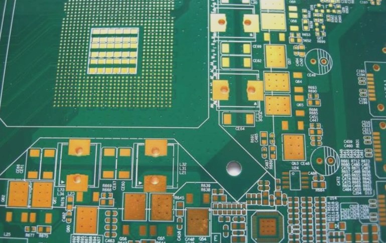
A via typically consists of a drill hole at its center and a surrounding pad area. Designers often opt for smaller vias in high-speed, high-density PCBs to maximize wiring space and reduce parasitic capacitance, ideal for high-speed circuits.
Parasitic Capacitance and Inductance of Vias:
Vias have parasitic capacitances and inductances that can impact circuit performance. The parasitic capacitance of a via can prolong signal rise time, while the parasitic inductance can weaken the filtering effect of the power system.
Calculations for parasitic capacitance and inductance can help designers understand their impact on signal integrity and circuit performance.
For example:
For a PCB board with specific dimensions, the parasitic capacitance of a via can be approximately calculated, influencing signal rise time.
Similarly, the parasitic inductance of a via can be calculated based on via length and hole diameter, affecting high-frequency current passage.
High-Speed PCB Via Design:
When designing high-speed PCB boards, careful consideration of via placement, size, and type is crucial to ensure optimal signal integrity and performance.

Optimizing Via Design for High-Speed PCB Boards
- Choose an appropriate via size, such as 10/20Mil for 6-10 layer memory module PCBs, or 8/18Mil for high-density small-sized boards, balancing cost and signal quality.
- Thinner PCB boards can help reduce parasitic parameters of vias.
- Avoid unnecessary vias to minimize signal trace layer changes.
- Place power and ground vias close to pins to reduce inductance and impedance.
- Add grounded vias near signal layer transitions for a short return path and consider reducing pad sizes in high-density via areas.
By implementing these design considerations, you can mitigate the negative effects of parasitic characteristics in high-speed PCB layouts, ensuring optimal signal integrity and performance.