A prototype arrives on your bench. It looks fine at a glance. Then you reflow it. Solder bridges appear between fine-pitch pads. A few vias with solder. Your debug time doubles.
I have seen this exact story many times. The root cause is often not the past. It is the solder resist. People ask me, “What is solder resist, and why does it matter so much?” It is the thin protective coating that blocks solder from wetting copper you did not intend to solder. It also protects copper from corrosion and handling damage.
This guide breaks the topic into practical pieces. You will learn which PCB solder resist material options exist. You will see key solder resist material property items that affect yield. I will also cover IPC-SM-840, how the mask is applied, and what “registration” really means in production. You will leave with design rules you can use today.
What Solder Resist Is and Why It Exists on Almost Every PCB
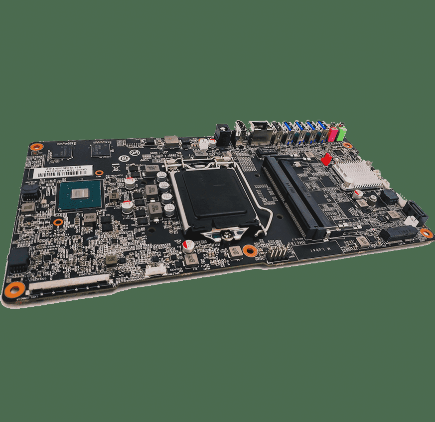
Solder resist is the insulating layer on top of the outer copper. Many engineers call it “solder mask.” In everyday PCB work, the two terms mean the same thing. The job is simple. It blocks solder from sticking where it should not stick.
Here’s what happens during assembly. Molten solder wants to wet exposed copper. If copper is exposed between pads, solder can bridge. A good mask creates a barrier between those pads. It leaves only the intended land areas open.
I still remember an early LED control board project. The layout used tight pad spacing. The assembler reported bridges on a connector footprint. We reviewed the Gerbers. The mask opening was too large. The copper gap was exposed. We reduced the opening and added mask dams. The bridging dropped right away on the next build.
This matters because a mask is not just “paint.” It is part of your electrical safety margin. It also supports long-term reliability in humid environments.
- Prevents solder bridging on fine-pitch parts.
- Reduces leakage paths from moisture and residue.
- Protects copper from scratches and oxidation.
- Improves cosmetic appearance and label contrast.
Key Functions That Affect Yield and Reliability
Most defects tied to the solder mask show up as assembly pain. Short circuits are the obvious ones. Hidden reliability issues are the expensive ones. I focus on four functions when I review a new design.
The first function is insulation. Solder mask has dielectric strength. It helps keep adjacent conductors isolated. This is critical when conductors run close together. It also helps when moisture sits on the surface.
The second function is solder control. Mask dams between pads reduce bridging risk. Dams between pads and vias reduce solder wicking. That helps with wave soldering and selective soldering too.
The third function is surface protection. Copper can corrode. Flux residue can be aggressive. A mask reduces exposure. It is not a full conformal coating, but it helps.
The fourth function is process visibility. Mask color and finish change how easy it is to inspect. Visual inspection still matters, even with AOI.
When teams skip mask reviews, the same problems appear.
- Pad openings that are too large for the pitch.
- Slivers of the mask that cannot be held during processing.
- Mis-registration that leaves copper exposed on one side.
- A mask on pads that causes poor wetting.
What “Solder Resist Material” Really Means in PCB Fabrication
People often ask about the exact chemistry. They ask “what is the material of solder” and assume the answer is similar for solder resist. These are different topics. Solder is a metal alloy. Solder resist is a polymer coating system.
In most factories today, the common solder resist is liquid photoimageable, or LPI. It is applied as a liquid ink. It is then exposed to UV light through the artwork. The exposed areas harden. The unexposed areas are developed away. The board is then fully cured.
This is where pcb solder resist material choice becomes real. Different masks have different resistance to heat, chemicals, and cracking. Different masks also behave differently during imaging. That affects fine features and registration stability.
Most engineers do not realize that mask behavior depends on the whole stack. Copper texture matters. Laminate type matters. Surface finish matters too. ENIG processing, for example, uses chemistry that can stress weak adhesion if the prep was poor.
I avoid oversimplifying material selection. A mask that works well on a simple 2-layer board may fail on a dense board with microvias. The right approach is to pick a qualified material, then validate on your design rules.
Core Solder Resist Material Properties You Should Check
When someone asks me for a “best solder mask,” I ask a different question. I ask which solder resist material property matters most for the product. The answer depends on the environment and assembly profile.
Here are the properties I check during quoting and DFM. I keep the language simple, but the impact is not simple.
- Adhesion. Poor adhesion can cause lifting during HASL, ENIG, or rework.
- Heat resistance. Lead-free reflow peaks are high. The mask must resist blistering.
- Chemical resistance. Plating and cleaning chemicals should not attack the mask.
- Electrical insulation. Higher insulation helps reduce leakage in wet conditions.
- Hardness and scratch resistance. Handling damage can expose copper.
- Color stability. Some colors show burn or discoloration after reflow.
Looking at the data sheets helps. Qualification to IPC-SM-840 also helps. It sets test methods and performance requirements. It does not guarantee perfect results. It does reduce risk.
Table: Practical property checklist for incoming material review
| Adhesion | Mask lifts near pads or edges | Leads to exposed copper and rework time |
| Thermal resistance | Blisters after lead-free reflow | Can cause latent shorts and cosmetic rejects |
| Chemical resistance | Soft or stained mask after wet processes | Impacts surface finish quality and reliability |
| Insulation performance | Leakage in humid tests | Matters for high-impedance and safety circuits |
| Hardness | Scratches from depanel or fixtures | Scratches can expose copper and invite corrosion |
Types of Solder Mask: LPI, Dry Film, Epoxy, and Peelable
Not every board uses the same mask type. The best choice depends on design and process. In high-mix production, LPI is the default. It supports fine lines. It also supports many colors.
A dry film photoimageable mask is used when a very uniform thickness is needed. It can help with some feature sets. It also has limits on conforming to topography.
Epoxy liquid masks exist, too. They can be used in some simpler flows. In modern fine-pitch work, they are less common than LPI.
A peelable mask is its own category. It is used to protect areas during soldering. After soldering, it is removed by hand. It is useful for edge connectors, test pads, and some through-hole zones. It is not meant as a permanent protective layer.
Table: Common solder mask types and when they fit
| LPI (liquid photoimageable) | Coat + UV image + develop + cure | Most commercial PCBs, fine-pitch SMT | Needs tight process control for registration |
| Dry film photoimageable | Lamination + UV image + develop | Uniform thickness needs on some builds | May struggle over rough topography |
| Epoxy liquid (non-photoimageable) | Screen print or coat with openings defined differently | Simple boards and some legacy processes | Less suited for tight features |
| Peelable mask | Printed and cured, then peeled off | Protect pads or holes during soldering | Labor to remove and area limits |
IPC-SM-840: The Standard That Keeps Material Claims Honest
IPC-SM-840 is the most referenced solder mask material standard. It defines qualification and performance requirements. It covers tests like adhesion, hardness, flammability, and environmental resistance. It also defines categories for different end-use expectations.
I use IPC-SM-840 as a baseline when I assess a supplier’s material system. It is not the only requirement. You still need process control. You also need workmanship standards in production. For assembly, J-STD-001 matters. For bare board acceptance, IPC-A-600 and IPC-6012 matter.
Here is a practical way to use IPC-SM-840 in procurement. Ask your PCB supplier which mask system they run. Ask if it is qualified to IPC-SM-840. Ask which class they built for your product. Also, ask how they control shelf life and storage.
I also advise buyers to align mask requirements with product risk. A consumer gadget has different needs than medical or avionics. If a product can harm people, you should push for tighter controls. You should also request traceability.
- Use IPC-SM-840 qualification as a supplier gate.
- Pair it with IPC-A-600 and IPC-6012 build class requirements.
- Confirm the factory’s process controls, not only the material name.
How Solder Mask Is Applied: Where Defects Are Born
The application method shapes the final result. The conventional flow is a photolithographic process. It has many steps. Each step can add risk if it is rushed.
Here is what happens in a typical LPI process. The board is cleaned. Oil and oxide are removed. The board is dried. Mask ink is coated. Coating can be done with screen coat or curtain coat. The mask is pre-baked to reduce tack. UV imaging defines the openings. The unexposed mask is developed away. Final curing hardens the coating.
Inkjet direct printing also exists. It can reduce waste. It can also simplify tooling. It is not ideal for every design. Your supplier should tell you what they run and why.
Thickness control matters. Being too thin can reduce insulation and durability. Too thick can cause poor definition around pads. Many fabricators control thickness through coating settings and viscosity checks. They also validate cure through process windows.
When a client faced random dewetting on pads, the mask was suspected. The root cause was poor cleaning before coating. The mask edge was ragged. Flux got trapped. We changed the cleaning parameters and added a surface energy check. The issue was reduced.
- Specify the mask type and color in fabrication notes.
- Ask how the supplier controls coating thickness and cure.
- Request coupon data if the project is high risk.
Solder Resist Registration: Why Alignment Is Harder Than It Looks
Solder resist registration means mask openings line up with the copper pads. It sounds simple. In production, it is a constant battle against tolerance stack-up.
Copper features can shift due to imaging. Laminate can move due to heat and moisture. Drill can wander within tolerance. Each step adds a small error. The mask image must land on the final copper position.
Here is what you see when registration is off. A pad is partly covered by a mask. Solder wetting drops. Tombstoning risk can rise on small passives. You may also see exposed copper beside pads. That can increase bridging risk.
Most teams do not budget enough clearance for mask alignment. They assume the same tolerance as copper etch. Mask registration is often less tight than copper imaging. You should ask your PCB shop for their stated mask registration capability. Then design to that number.
I like to review every fine-pitch footprint with the fabricator’s DFM rules. This is where a calm conversation saves weeks. WellCircuits has done this kind of review with many buyers. A short DFM call often prevents a long rework loop.
DFM Rules That Prevent the Most Solder Mask Problems
Mask DFM is about avoiding shapes that the process cannot hold. Slivers are a classic trap. A sliver is a very thin strip of material between openings. If it is too thin, it will not survive development and cure. It may break off and expose copper.
Via strategy also matters. A “tented via” is covered by a mask. Only the annular ring is covered. If the hole is sealed fully, it is called plugged or filled, depending on the method. Tenting is popular because it is cheaper. It is not always reliable for larger vias. It also depends on the soldering method.
Here are four DFM guidelines I use often. They are not universal. Your supplier’s process window still rules.
- Avoid tiny mask dams on very fine pitch. Use solder mask defined pads only when needed.
- Decide via tenting early. Tented vias reduce solder wicking. They can trap air in some cases.
- Control mask expansion. Oversized openings expose copper. Undersized openings cover pads.
- Call out special areas. Edge connectors and test pads may need a peelable mask or no mask.
Think about your assembly flow, too. Wave soldering needs a different mask strategy than reflow only. Selective soldering has its own rules. If you share that process info, the DFM feedback gets sharper.
Why Green Is Common, and When Other Colors Make Sense
Green solder resist became standard for practical reasons. It gives a strong contrast with copper and white silkscreen. It is easy on inspectors’ eyes during long shifts. It also works well with UV imaging in many lines.
Other colors can be used. Black can look premium. It can also hide defects during inspection. White can be useful for LED boards. It can also discolor with heat if the system is not tuned. Red and blue are popular for branding and visibility. Some shops report that certain colors image more sharply in their process. The effect depends on the specific ink system and exposure settings.
Color choice should not be only about appearance. You should ask about lead time and cost. Green is often cheaper because it is run more. Some special colors add process steps. Some also reduce yield on tight features.
If you need a custom color for a product line, I suggest a small pilot build. Measure assembly yield. Inspect for registration stability. Then lock the spec.
How to Choose a Solder Mask Spec That Survives Scale-Up
Prototype success can hide future issues. A lab build may use careful hand soldering. Mass production uses fast reflow and high-volume inspection. Mask defects become more expensive at scale.
I recommend writing a simple, clear mask spec in your fab notes. Include mask type, color, and any keep-out needs. Call out peelable mask zones if required. Align the spec with your acceptance standard. IPC-A-600 is a common reference for visual acceptance. IPC-6012 sets performance requirements for rigid boards.
You should also decide what you will not accept. If you need tight mask registration, say so. If you cannot tolerate exposed copper near high-voltage nets, call it out. If you need traceability, request it.
This is also where transparency matters from the supplier side. A good shop will tell you the limits. They should not promise impossible dams on a 3 mil pitch without proof. If your design is on the edge, ask for a capability review and a test coupon.
If you want a second set of eyes, ask for a DFM review before ordering. That is often the cheapest quality insurance you can buy.
Frequently Asked Questions
Are solder mask and solder resist the same thing?
In most PCB discussions, yes. Both terms describe the protective coating that blocks solder from wetting unwanted copper. Some documents prefer one term. Factories and designers often mix them. What matters is the spec you provide. Call out the mask type, color, and any special areas.
What is solder resist, in one sentence?
Solder resist is an insulating coating on a PCB that leaves only selected pads exposed for soldering. It reduces bridging and protects copper. It also improves handling durability. It is not the same as conformal coating, which is added after assembly.
What is the material of solder, and does it relate to solder mask?
Solder is a metal alloy. Common electronics solders are tin-based alloys, such as SAC alloys for lead-free work. Their solder material properties include melting range, wetting, and joint strength. Solder mask is not metal. It is a polymer coating designed for insulation and solder control.
Does solder mask color change performance?
Sometimes, but it depends on the ink system and the process window. Green is common because it images and inspects well in many factories. Other colors can work well too. The risk is usually inspection difficulty, yield, and lead time. If your design is dense, validate the color choice with a pilot run.
What is solder resist registration, and why should I care?
Solder resist registration is the alignment of mask openings to copper pads and features. Poor alignment can cover pads or expose copper near pads. That can cause poor soldering or bridging. Registration depends on material movement and process tolerances. Your design should allow clearance for real factory capability.
When should I use peelable solder mask?
Use a peelable mask when you must protect an area during soldering, then expose it later. Common examples are test points and some through-hole zones. It is removed by hand after soldering. It is not meant for permanent protection. Large holes and large areas may need polyimide tape instead.
Which standards matter most for solder mask quality?
IPC-SM-840 is the key material standard for solder mask qualification. IPC-A-600 covers acceptability for bare boards. IPC-6012 covers performance and qualification for rigid boards. Assembly workmanship is covered by J-STD-001. Use these together for a complete quality framework.
Conclusion
Solder resist looks like a simple layer, but it controls many failure modes. I have watched one small mask opening change turn a painful build into a stable one. The best results come from treating the mask as a real design feature. It is not an afterthought.
Use IPC-SM-840 as a baseline. Ask about process controls and registration capability. Review fine-pitch footprints and via strategy early. If you want help, request a quick DFM and mask review with your PCB partner. If your team needs that extra check before release, WellCircuits can review the mask rules and highlight risks before fabrication.