ELIC HDI PCB


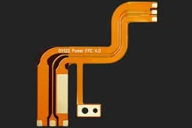
6 Layer HDI Flex PCB

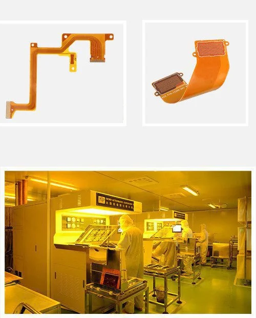
HDI Flex PCB
4L 1 Tier HDI PCB
6L 2 Tier HDI PCB
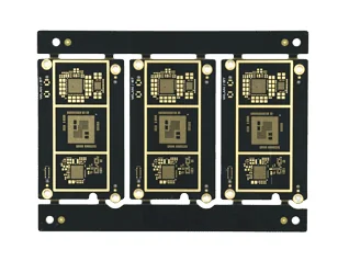
8L 2 Tier HDI PCB
HDI Flex PCB
Layer:6L 2 Tier
Thickness:1.3mm
Size:118.29mm*113.12mm
Min blind vias:0.1mm
Min buried vias:0.2mm
Min Trace:0.084mm
Min Space:0.089mm
Finish:ENIG+OSP
4L 1 Tier HDI PCB

Layer:4L 1 Tier
Thickness:0.8mm
Size:70mm*86mm
Min Trace:0.12mm Min Space:0.075m
Min Hole Size:0.1m
Finish:ENIG+0SP
Application: Smart Watch
6L 2 Tier HDI PCB

Layer:6L 2 Tier
Thickness:1.0mm
Size:92mm*118mm
Min Trace:0.075mm
Min Space:0.075mm
Min Hole:0.1mm
Finish:ENIG
Application: Mobile Phone
8L 2 Tier HDI PCB
 Layer:8L 2 Tier
Thickness:1.0mm
Size:118.29mm*113.12mm
Min blind vias:0.1mm
Min buried vias:0.2mm
Min Trace:0.084mm
Min Space:0.089mm
Finish:ENIG+OSP
Application: Car DVR

Need a Quote?
Fill in your requirements and get a detailed quotation within 24 hours.
Request a QuoteNo account required • Free consultation
Request a Quote
Fill in your requirements and we'll get back to you within 24 hours.