

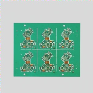
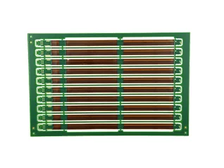
4-layer HDI first-level RF combination PCB
The 4-layer HDI first-level RF combination PCB from WellCircuits represents a pinnacle of flexible circuit engineering, designed for demanding applications requiring both high-density interconnect (HDI) and integrated radio frequency (RF) performance. As a flexible printed circuit board (FPC), it offers exceptional form factor flexibility, enabling miniaturization and dynamic movement in complex designs. Manufactured in our ISO 9001-certified facility, this product is meticulously crafted to meet stringent IPC Class 2 or Class 3 standards, making it ideal for engineers and procurement managers seeking reliable, high-performance solutions for advanced consumer electronics, automotive systems, and medical devices.
Key Specifications
WellCircuits specializes in manufacturing custom PCBs to your exact specifications. Below are typical capabilities for our 4-layer HDI first-level RF combination PCBs. Specific requirements can be discussed during the quotation process to ensure optimal performance and manufacturability.
| Specification | Typical Capability / Value | Notes |
|---|---|---|
| Layer Count | 4 Layers | Designed for complex routing and signal integrity. |
| Board Type | Flexible PCB (FPC) with RF integration | Utilizes polyimide (PI) for flexibility; specific RF dielectrics for controlled impedance. |
| Base Material (Flex) | Polyimide (PI) Film, Adhesive-less or Adhesiveless Copper Clad Laminate | High thermal stability, excellent flexibility. |
| RF Dielectric Options | Low-loss PI, LCP (Liquid Crystal Polymer), or specialized RF laminates (e.g., Rogers, Taconic) | Selected based on frequency, Dk/Df requirements for optimal RF performance. |
| Board Thickness | 0.15mm – 0.4mm (Finished Board) | Dependent on layer stack-up and material selection. |
| Minimum Line Width/Spacing | 2/2 mil (0.05mm) | Achieved with advanced HDI manufacturing processes. |
| Minimum Drill Size (Mechanical) | 6 mil (0.15mm) | For conventional through-hole vias. |
| Minimum Laser Drill (Microvia) | 2 mil (0.05mm) | Essential for HDI and advanced interconnect density. |
| Aspect Ratio (Mechanical Drill) | Up to 10:1 | Ensures reliable plating for through-hole vias. |
| Aspect Ratio (Microvia) | 1:1 | Standard for laser-drilled microvias. |
| Controlled Impedance Tolerance | ±5% (Standard), ±3% (High Precision) | Critical for RF signal integrity, verified by TDR testing. |
| Surface Finish Options | ENIG (Electroless Nickel Immersion Gold), ENEPIG (Electroless Nickel Electroless Palladium Immersion Gold), Immersion Silver, OSP (Organic Solderability Preservative) | ENIG/ENEPIG recommended for RF and fine-pitch components. |
| Solder Mask / Coverlay | Polyimide Coverlay, Liquid Photoimageable Solder Mask (LPI) | Offers protection and defines solderable areas. |
| Outline Tolerance | ±0.1mm (Routing), ±0.05mm (Laser Cutting) | Ensures precise fit and assembly. |
| Copper Weight | 0.5 oz – 1 oz (Outer Layers), 0.5 oz – 1 oz (Inner Layers) | Customizable based on current carrying and impedance requirements. |
| Thermal Management | Optional thermal vias, heatsink attachment pads | For designs with high power dissipation. |
| IPC Compliance | IPC Class 2 or IPC Class 3 | Specify at order for desired reliability level (referencing IPC-6012 for fabrication and IPC-A-610 for assembly acceptability). |
| Quality Control | 100% AOI (Automated Optical Inspection), 100% Electrical Test, X-ray Inspection | Ensures defect-free and functional boards. |
Applications
The unique combination of HDI and RF capabilities in a flexible format makes this PCB ideal for groundbreaking products across various industries:
- Smartphones & Wearables: Enabling compact designs for 5G/6G antennas, NFC modules, and high-frequency sensors.
- Automotive Electronics: Crucial for ADAS (Advanced Driver-Assistance Systems) radar modules, in-cabin connectivity, and flexible sensor arrays that can conform to vehicle contours, meeting AEC-Q100/Q200 standards.
- Medical Devices: Essential for miniature diagnostic tools, flexible surgical instruments, and wearable health monitors requiring high-frequency signal processing and ergonomic integration.
- Aerospace & Defense: For lightweight, robust communication systems, radar components, and sensor networks in space-constrained environments.
- IoT & Smart Devices: Integrating high-frequency wireless communication (Wi-Fi 6E, mmWave) and complex data processing into smaller, more flexible form factors.
- Telecommunications Infrastructure: Supporting next-generation network equipment, small cells, and antenna arrays where space and performance are critical.
Why Choose WellCircuits?
- Uncompromising Quality: Our manufacturing processes are guided by an ISO 9001:2015 certified quality management system, with a defect escape rate consistently below 0.5%. Every board undergoes rigorous inspection, including 100% Automated Optical Inspection (AOI) and electrical testing, ensuring compliance with IPC-A-600 and IPC-A-610 standards for acceptability.
- Advanced RF & HDI Expertise: We possess deep knowledge and state-of-the-art equipment for handling complex HDI structures, microvias, and precise impedance control, critical for first-level RF integration. Our engineers are proficient in IPC-2221 and IPC-2223 (for flexible circuits) design guidelines, providing valuable DFM (Design for Manufacturability) support.
- Reliability for Demanding Environments: Offering builds compliant with IPC Class 2 for general electronics and IPC Class 3 for high-reliability applications, including those requiring automotive-grade robustness (AEC-Q100/Q200 for component-level stress testing, which influences PCB design and material selection).
- Dedicated Support & Fast Turnaround: From initial design review to final production, our team provides expert guidance. We offer competitive lead times, with standard sample production in 3-5 working days and mass production typically within 5-15 working days, depending on complexity and volume.
Pricing & Lead Time
Due to the custom nature and advanced specifications of 4-layer HDI first-level RF combination PCBs, pricing is determined by design complexity, material selection, quantity, and specific testing requirements. WellCircuits offers competitive pricing and flexible volume options, from prototyping to high-volume mass production.
Our typical lead times are:
- Sample Lead Time: 3-5 working days
- Mass Production Lead Time: 5-15 working days
For an accurate quote and detailed lead time tailored to your project, please contact our sales team with your Gerber files and specifications.
{"@context":"https://schema.org","@graph":[{"@type":"TechArticle","@id":"https://www.wellcircuits.com/pcb-product/4-layer-hdi-first-level-soft-hard-combination/#techarticle","headline":"4-layer HDI first-level RF combination PCB","description":"4 layer HDI first level RF combination PCB: Learn about 4 layer hdi first level rf combination pcb specifications, applications, and manufacturing capabiliti...","url":"https://www.wellcircuits.com/pcb-product/4-layer-hdi-first-level-soft-hard-combination/","inLanguage":"en-US","isPartOf":{"@id":"https://www.wellcircuits.com/pcb-product/4-layer-hdi-first-level-soft-hard-combination/#webpage"},"author":{"@type":"Person","@id":"http://www.wellcircuits.com/#/schema/person/1","name":"even","url":"http://www.wellcircuits.com"},"publisher":{"@id":"http://www.wellcircuits.com/#organization"},"datePublished":"2024-10-29T11:07:32+08:00","dateModified":"2026-06-24T12:05:26+08:00","image":{"@id":"https://cdn.wellcircuits.com/wp-content/uploads/2024/10/20240130111948_14.webp"}},{"@type":"QAPage","@id":"https://www.wellcircuits.com/pcb-product/4-layer-hdi-first-level-soft-hard-combination/#qapage","mainEntity":{"@id":"https://www.wellcircuits.com/pcb-product/4-layer-hdi-first-level-soft-hard-combination/#techarticle"}},{"@type":"Organization","@id":"http://www.wellcircuits.com/#organization","name":"WellCircuits","url":"http://www.wellcircuits.com","logo":{"@type":"ImageObject","url":"https://cdn.wellcircuits.com/wp-content/uploads/2025/03/wellcircuits-logo.png"}},{"@type":"Person","@id":"http://www.wellcircuits.com/#/schema/person/1","name":"even","url":"http://www.wellcircuits.com","jobTitle":"PCB Manufacturing Engineer","worksFor":{"@id":"http://www.wellcircuits.com/#organization"}}]}
Need a Quote?
Fill in your requirements and get a detailed quotation within 24 hours.
Request a QuoteNo account required • Free consultation
Request a Quote
Fill in your requirements and we'll get back to you within 24 hours.