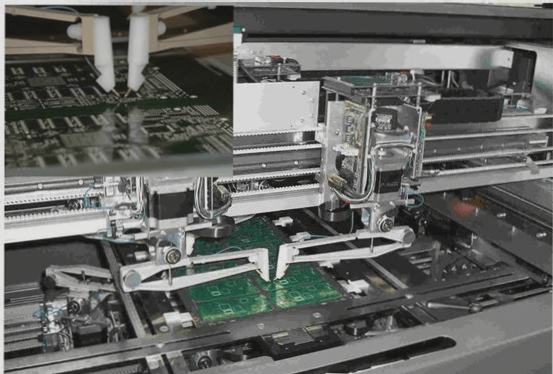
PCB Online Test Fixture Design Rules for Cost and Complexity Reduction
- 1. Ensure the test pad diameter for probe testing is at least 0.9 mm, proportional to the hole size.
- 2. Maintain a clearance around the test probe at 80% of adjacent component height, with a minimum of 0.6 mm.
- 3. Limit component height on the test surface to 5.7 mm and keep test pads at least 5 mm away from high components.
- 4. Avoid placing components or test pads within 3 mm from the edge of the circuit board.
- 5. Apply flux or conductive non-oxidizing coating to all probe areas; avoid solder mask on test pads.
- 6. Ensure probe contact point is on the pad, not the end point, especially for leadless SMT component arrays.
- 7. Use probes to test both sides of the board; switch test points with through-holes for reliability.
- 8. Prefer standard probes with the center hole of the test pad set at 2.5 mm for reliability.
- 9. Minimize gold fingers as test pads to prevent damage from test probes.
- 10. Distribute test pads evenly across the board to prevent bending and probe failure.
New Information:
Recent advancements in PCB testing have introduced the concept of using AI algorithms to optimize test pad distribution for increased efficiency. By analyzing historical test data and component layouts, AI can suggest ideal test pad locations to further enhance testing accuracy and reduce fixture setup time.
Furthermore, the integration of IoT technology into test fixtures allows for real-time monitoring of test parameters, enabling manufacturers to identify and address potential issues promptly, leading to improved overall product quality.