PCB Fabrication Process Guide
Introduction to PCB Fabrication
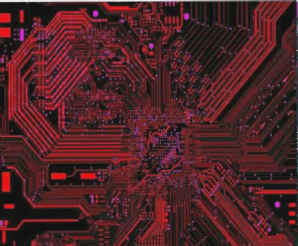
In today’s technology-driven world, understanding PCBs is essential. Explore the PCB fabrication process and its significance in the electronic industry.
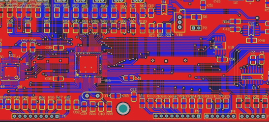
Types of PCBs
- Single-layer
- Double-layer
- Multi-layered
The fabrication process for each type is similar, involving steps like layout creation, etching, drilling, and more.
Key Steps in PCB Fabrication
- PCB Layout Design
- PCB Manufacturing
- PCB Inspection
- PCBA (PCB Assembly)
Each step, from layout design to final assembly, plays a crucial role in ensuring the functionality of electronic devices.
Specialized Techniques in PCB Fabrication
- PCB Designing
- Production Preparation
- Inner Layer Etching
- AOI of Inner Layer
- Lamination
- Drilling
- Electroless Copper Deposition
- Horizontal Electrolytic Plating
- Outer Layer Imaging
- Graphic Plating
- Outer Layer Etching
- Solder Mask Application
- Silkscreen Printing
- Surface Finish
- Electrical Testing
- Packaging and Delivery
These steps outline the intricate process of PCB fabrication, emphasizing the importance of precision and expertise in the industry.
Conclusion
Understanding PCB fabrication is crucial for ensuring the quality and performance of electronic devices. For optimal results, consult experienced PCB manufacturers for expert guidance and support.
Enhanced Content for PCB Experts
As a top-notch PCB specialist, it’s crucial to stay updated on the latest industry trends and advancements. Here are some key insights to keep you informed:
- 1. The Importance of High-Frequency PCB Design Techniques
- 2. Implementing Advanced Thermal Management Strategies in PCBs
- 3. The Rise of Flexible and Rigid-Flex PCB Technologies
- 4. Integrating IoT Capabilities into PCB Development
By staying abreast of these developments, you can enhance your expertise and stay ahead in the ever-evolving world of PCB design.