Benefits of PCB Layering and Structure
- When to Consider Adding Layers to PCB Routing
- Understanding Core Structure vs. Foil Structure in PCBs
- Importance of Balanced Stack-Up in PCB Design
1. Why Add Extra Layers to PCBs?
While reducing layers can make PCBs thinner, adding layers may actually reduce costs in some cases. The decision depends on factors like cost and flexural characteristics.
2. Core vs. Foil Structure
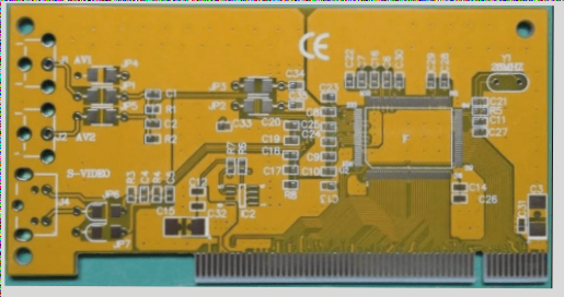
PCBs have two main structural types: core structure embeds all conductive layers within the core material, while foil structure uses a foil dielectric board for outer conductive layers.
3. Achieving Balance in PCB Design
Balancing the structure of PCBs is crucial to prevent bending and ensure quality. Strategies like using uniform signal layers and introducing blank signal layers can help achieve a balanced stack-up.
Cost Advantage of Uniform PCB Boards
Odd-layered PCBs may have lower raw material costs but higher processing costs compared to even-layered PCBs. The processing cost for outer layers in odd-layered PCBs is notably higher due to non-standard bonding processes.
Balancing the Structure to Prevent Bending
Preventing PCB bending is essential for efficiency and cost-effectiveness. Achieving a balanced stack-up is key to avoiding warping during cooling phases and maintaining production quality.
Solving PCB Layout Issues for DC/DC Converters
Strategies like using uniform signal layers, adding extra power layers, and introducing blank signal layers can help address PCB layout challenges, reduce costs, and improve overall quality.
If you have any questions about PCBs, feel free to contact us at info@wellcircuits.com.