Ion Migration in Electroplating
When an electric field is applied, ions in the electroplating solution undergo ion migration due to electrostatic forces. This migration rate can be calculated using the formula: u = zeoE/6πrη. Here, u represents the ion migration rate, z is the ion’s charge number, eo is the charge of an electron (1.61019C), E is the potential, r is the radius of the hydrated ion, and η is the solution’s viscosity. A higher potential drop and lower solution viscosity lead to faster ion migration.
Electrodeposition Theory
During electroplating, the printed circuit board on the cathode acts as a non-ideal polarized electrode. Copper ions on the cathode’s surface gain electrons, reducing them to copper atoms and increasing the copper ion concentration near the cathode. This creates a copper ion concentration gradient, with a diffusion layer forming around the cathode. The COTTRELL equation, I = zFACbD/πrηCo, relates the current to factors like charge number, surface area, diffusion coefficient, and ion concentrations.
Limiting Diffusion Current
The limiting diffusion current, ii, depends on the main plating solution’s copper ion concentration, diffusion coefficient, and diffusion layer thickness. Higher copper ion concentration, larger diffusion coefficient, and thinner diffusion layer result in a larger limiting diffusion current. To increase this current, technological measures like heating can be employed to enhance diffusion coefficient and convection rate, achieving a faster plating rate.
Horizontal Electroplating
Horizontal electroplating systems utilize accelerated convection speeds to form eddy currents in the plating solution, reducing the diffusion layer thickness to around 10 microns. This allows for high current densities up to 8A/dm2, making the plating process more efficient.
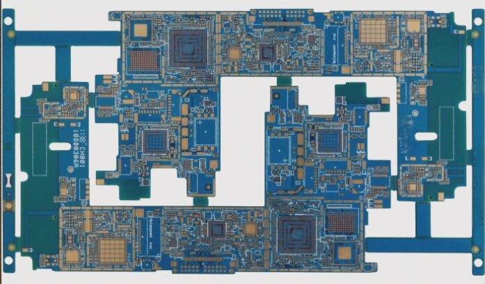
The Importance of PCB Electroplating for Uniform Copper Layer Thickness
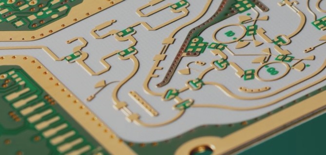
One of the critical aspects of PCB fabrication is ensuring the uniformity of the copper layer thickness on both sides of the substrate and within via holes. Achieving this uniformity requires maintaining a fast and consistent flow rate of the plating solution.
In a horizontal electroplating system, the strategic placement of nozzles allows for the quick and vertical spraying of the plating solution onto the board, accelerating its flow through the via holes. This rapid flow creates eddy currents that help reduce the diffusion layer, leading to a more uniform coating.
However, challenges arise when the plating solution enters narrow through-holes, causing reverse reflow and uneven copper layer thickness. To address this, adjusting controllable process parameters based on the board’s aspect ratio and using high-dispersion copper electroplating solutions with additives can help achieve uniform plating thickness.
Furthermore, as the demand for micro-blind holes increases, incorporating ultrasonic vibration during electroplating becomes essential to enhance solution replacement and circulation within these tiny holes. By fine-tuning parameters and utilizing innovative techniques like reverse pulse current, a high-quality copper coating with excellent distribution capabilities can be achieved.
Through meticulous process testing and adjustment, satisfactory results in controlling the uniformity of copper electroplating thickness on printed circuit boards can be attained.