Understanding Gold Finger Connectors in PCBs
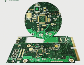
Gold fingers are specialized connectors located at the edge of a printed circuit board (PCB). These connectors, shaped like fingers, play a crucial role in protecting PCB prototypes from wear and tear. Check out the image below for a visual representation:

Surface Treatments for Gold Finger PCBs
Electroplated Nickel Gold: This treatment, with a thickness ranging from 3-50 microns, offers excellent conductivity, oxidation resistance, and wear resistance. It is ideal for gold finger PCBs subjected to frequent insertion and mechanical friction.
Immersion Gold: With a typical thickness of 1 micron (up to 3 microns), immersion gold is widely used in high-precision PCBs for its superior conductivity, flatness, and solderability. The cost-effective process results in a golden yellow finish.
Design Tips for Gold Finger PCBs
When designing a PCB similar to the example below, look out for gold fingers indicated by pins and a U-shaped groove on both the TOP and BOTTOM sides:

Here are some key design considerations for gold finger processing:
- For PCBs requiring frequent insertion, opt for hard gold plating on gold fingers for enhanced wear resistance.
- Chamfer the gold finger at a 45° angle to prevent issues; see example below:
- Apply a solder mask window treatment to the gold finger area.
- Maintain a minimum distance of 14 mils from the tip of the gold finger for immersion tin and silver pads.
- Avoid placing copper directly on the gold finger surface.

For a well-designed gold finger reference, check out the image below:

- Ensure all inner layers beneath the gold finger have copper cutting to reduce impedance differences and aid in ESD protection.
- Consider full copper cutting beneath the gold finger pad for optimal performance.
Important Considerations for PCB Gold Fingers Processing and Production
- PCBs with thickness ranging from 1.2 mm to 2.4 mm can undergo processing with a beveled edge. Boards outside this thickness range are not suitable for this method.
- The bevel angle typically falls between 20° and 45°. It is crucial to maintain a sufficient distance between the gold finger and the board edge. Depending on the PCB design or thickness, it is recommended to have a distance of 0.6 mm to 1.5 mm to prevent gold finger damage.
Here are some common diagrams showcasing various bevel angles and depths for your reference:


If you have any inquiries about PCBs or PCBA, please don’t hesitate to contact me at info@wellcircuits.com.