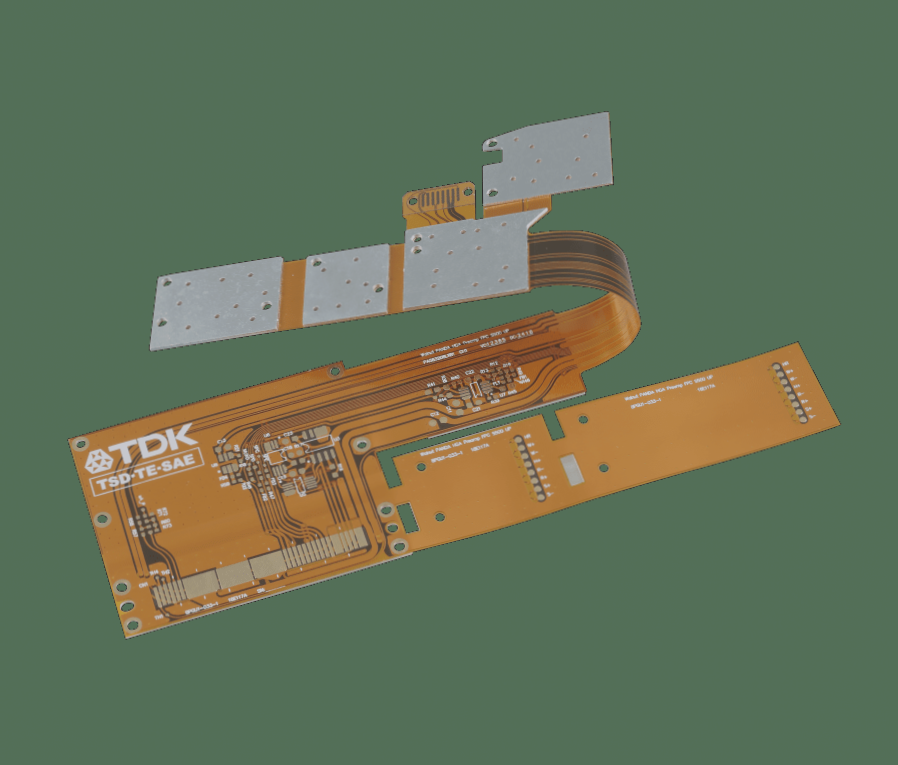
PCB Fabrication and Electroplating Technologies
PCB applications span various industries, from aviation to household electronics, relying on copper connections for conductivity. Prolonged exposure to air can lead to oxidation and corrosion, impacting solderability. To protect circuit boards, specialized technologies are essential.
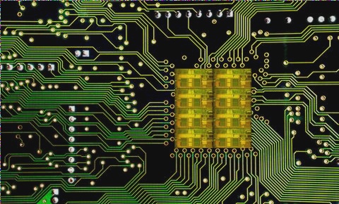
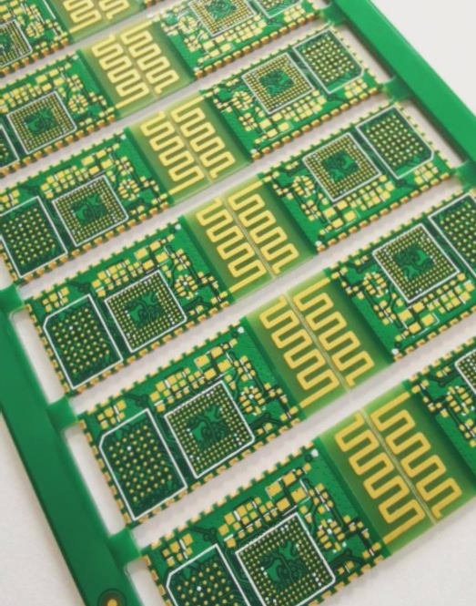
The PCB electroplating process involves several key steps, including acid treatment, copper plating, pattern transfer, degreasing, rinsing, etching, tin plating, and more. Three main electroplating technologies—oxide film, organic coating, and electroplating—offer distinct advantages, with electroplating being the preferred choice for most manufacturers.
Distinguishing PCB Electroplating Processes
- Oxide Film:
- Organic Coating:
- Electroplating:
Common Challenges in Electroplating
- Issues with Chrome Plating Layer: Brown films may form due to sulfate concentration, low temperature, or impurities like Cl-.
- Coating Peeling: Inadequate pre-plating processes can cause coating peeling after nickel and chromium plating.
- Bright Nickel Plating Concerns: Contamination from impurities in raw materials or improper cleaning processes can lead to harmful decomposition products and require careful elimination.
By addressing these challenges and understanding the nuances of different electroplating technologies, manufacturers can enhance the quality and reliability of PCBs.