PCB Design in Industrial Applications
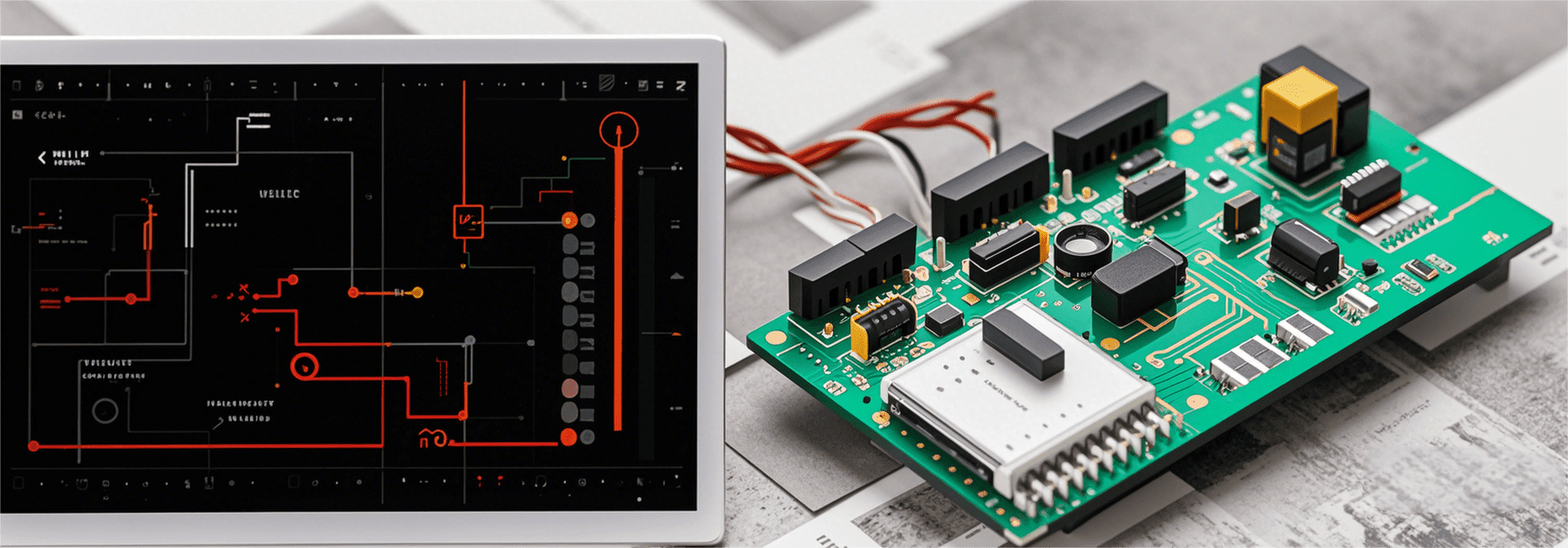
Understanding pcb design basics is essential for anyone looking to create reliable and high-performance electronic products. PCB design is a critical process that enables the creation of electronic circuits tailored to specific customer requirements. Engineers design PCB schematics to fulfill the functional tasks outlined by customers. The primary tasks in PCB design include:
Schematic Design: Creating a detailed diagram of the electronic components and their interconnections. This step involves schematic capture, where schematic symbols are used to represent components and single nets define individual electrical connections, forming the foundation before moving to layout. PCB design is inherently multidisciplinary, integrating principles of electrical engineering—from schematic creation to hardware realization—with electrical engineers playing a key role in ensuring the design meets both functional and technical requirements.
Layout Considerations: Board layout is a key part of the design process, involving the arrangement of external connections and the overall shape and structure of the product. Optimizing board layout is essential for efficient placement, routing, and validation. Component Placement: Optimal placement of electronic components within the PCB for performance and space efficiency. The board outline defines the physical boundaries for placing components, and accurate placement is crucial for optimal performance and manufacturability.
Circuit Connections and Via Holes: Optimizing the layout of circuit connections and via holes for signal integrity and manufacturing ease. Electromagnetic Protection and Heat Dissipation: Ensuring EMI protection and effective heat dissipation for reliable operation.
A PCB is built on a non conductive substrate, often a rigid substrate such as FR-4, which provides structural stability. The vast majority of PCBs use this type of base material. Copper layers and copper traces are then added to form the electrical pathways, while insulating material separates these layers to maintain signal integrity and mechanical stability. In advanced designs, multiple layers, extra layers, and alternating layers are used to achieve complex circuitry and enhance performance.
An excellent PCB design not only reduces manufacturing costs but also enhances the performance and reliability of electronic products. This is particularly important in industries such as aerospace, automotive, the Internet of Things (IoT), consumer electronics, medical, and telecommunications.
Applications in Specific Industries
Aerospace: PCBs must withstand extreme conditions and provide high reliability. They are used in satellite systems, aerospace communication equipment, and other critical components. Designing for harsh environments requires careful consideration of physical requirements and mechanical components.
Automotive: PCBs are integral to modern vehicles, supporting advanced features like infotainment systems, engine management, and safety systems. They must meet stringent requirements for performance and reliability.
IoT: IoT devices require compact and efficient PCB designs to support wireless connectivity and low power consumption. Flexible and rigid-flex PCBs are often used to accommodate the diverse form factors of IoT devices.
Consumer Electronics: PCB design in this sector focuses on miniaturization, flexibility, and wireless connectivity. High-density interconnect (HDI) and flexible PCBs are commonly used to create compact and portable devices like smartphones and wearables.
Medical: Medical PCBs are crucial for diagnostic equipment, patient monitoring devices, and therapeutic equipment. They must comply with stringent regulations and ensure high reliability and precision. Surface Mount Technology (SMT) is often preferred for its compactness and efficiency.
Telecommunications: PCBs in telecommunications must handle high-frequency signals and maintain signal integrity. They are used in mobile devices, base stations, and optical networking equipment, with a focus on miniaturization and high-performance materials.
WellCircuits’ PCB Design Services
WellCircuits offers comprehensive PCB design services to help customers accelerate their time-to-market. Our engineering team has extensive experience in designing PCBs for various industries, including aerospace, automotive, medical, telecommunications, and consumer electronics.
What is PCB Design?
Concept to Design Document: Whether you have an idea, a concept, or a completed schematic, we can transform it into a detailed design document, followed by PCB manufacturing, assembly, and testing. With over 15 years of experience, we ensure that the design meets all production requirements.
Collaborative Development Process: Our PCB design team works closely with you throughout the product development process, ensuring that all design aspects are technically reviewed before the first production run. Typically created mechanical definitions and constraints are considered to ensure the design meets all physical requirements.
Rapid Prototyping: Once the PCB design is approved for production, our skilled production team is ready to build high-quality PCBA prototypes for initial testing and development purposes.
Efficient Assembly: We offer both machine and hand placement options, allowing for PCB assembly in as little as 48 hours, with full inspection as standard and additional tests available upon request. In certain applications, through hole components are used for their reliability and ease of manual assembly.
Seamless Service Integration: By providing all these services under one roof, WellCircuits streamlines the process, saving you valuable time and allowing you to focus on delivering your product to market.
WellCircuits’s circuit board design – A perfect “layout” electronic art for you
Based on circuit board design and PCB prototype fabrication services, actively build PWB design, PCB manufacturing, SMT chip, material one-stop PCB Assembly business.
Senior PCB design and PCB layout team
More than 15 years of professional design experience, from PCB board design to PCBA manufacturing to provide solutions. The best circuit board design is “design quality” + “cost control” + “debugging convenience”.
High difficulty printed circuit board design experience
Good at high-frequency PCB, high-speed PCB, high-density PCB, mixed digital and analog, high power, high current, RF PCB, ate PCB, Rigid-Flex PCB, a high-speed backplane, etc. 2000 + PCB board design experience every year.
Rich technical resources
Chip companies cooperate early, accumulate forward-looking technology, synchronize cutting-edge technology, master the most advanced technical information, and fully consider EMI, EMC, and manufacturability design.
High-quality management system
Standardized design management system, strict inspection, level by level, do not let go of any mistakes and details, to ensure that the failure rate is zero, 10000 + customers account monument accumulation.
High standard security measures
High standard confidentiality measures, signed a confidentiality agreement, the company’s designer computer fully encrypted, the export of documents need to be fully approved, to ensure that the documents are 100% confidential.
Quality: perfect “design guide” and “design specification” provide additional technical suggestions beyond PCB layout, first-class training system, and training platform.
Self-inspection:self-inspection layout, wiring, rules, aesthetics, thermal design structure, etc
Review:WellCircuits senior team participate in the study together, from the schematic design, DFM, DFT, high speed, EMC, thermal design, and other comprehensive checks and mutual inspection
Mutual inspection: the best way to avoid personal thinking set, brainstorm, standardized and strictly controlled joint inspection system, perfect DFM review process
PCB board design software
Protel, PROTEL 99SE, PROTEL DXP, and Altium are primarily used in China. These are software developed and upgraded by a company. The current version is Altium designer 15, which is relatively random and straightforward in design, but it is not very good to make complex PCB software. However, it offers essential pcb design features and a user-friendly user interface for basic projects.
Cadence SPB software cadence SPB this is cadence’s software, and the current version is cadence SPB 16.5; OrCAD schematic design is an international standard; PCB board design and simulation are complete, which is more complex than Protel, mainly due to complex requirements and settings; However, it has made provisions for the design, so the design gets twice the result with half the effort, which is more potent than Protel.
Bordstationg and ee of mentor company, among which, since word station is only applicable to a UNIX system, it is not designed for PC, so few people use it; The current version of mentor EE is mentor EE 7.9 and cadence SPB, which belong to the same level of PWB design software. It is worse than cadence SPB in some places. Its strengths are stay wire and flying wire, which is called the king of flying wire.
Eagle circuit board design for easy layout is the most widely used printed circuit board design software in Europe. The above-mentioned PWB design software is widely used. Cadence SPB and mentor are well-deserved kings. If you are a beginner in circuit board design, I think cadence SPB is better. It can give designers a good design habit and ensure good design quality.
PCB editor and pcb design tools play a crucial role in the design and layout process, providing advanced features and an intuitive user interface to handle complex designs. Modern tools like Autodesk Fusion offer integrated workflows for both electrical and mechanical design, setting them apart from other software by enabling earlier collaboration and saving significant time.
How to design PCB board? Four Stages of PCB Design
Refine the concept.–We summarize the objectives of the project and create a document to specify the project’s technical scope.
Feasibility Study.–We conduct a study to examine whether the project will be possible within the client’s budget. Agreed terms of reference will be set out. A draft report is presented to the client for feedback.
Hardware and Software Design.–We design the electronic circuit and produce the schematic designs, manufacturing bench-top prototypes. Software code is drafted.
Test and trials.–When software and hardware designs are complete we can begin serious bench testing. We continue until the design meets the project specifications.
Pre-preparation
Includes preparation of component libraries and schematics. Before circuit board design, the schematic SCH component library and PCB component packaging library should be prepared first.
The PCB component package library is best built by the engineer according to the standard size data of the selected device. In principle, the component packaging library of PC is first established, and then the schematic SCH component library is established.
The requirement of a PCB component packaging library is high, which directly affects the installation of PCB. Schematic SCH component library requirements are relatively loose but pay attention to the definition of pin properties and the corresponding relationship with the PCB component packaging library.
PCB structure design
According to the size of the circuit board and the mechanical positioning, draw the PCB frame in the PCB board design environment, and place the required connectors, buttons/switches, screw holes, assembly holes, etc. according to the positioning requirements. Fully consider and determine the wiring area and the non-wiring area (how much area around the screw hole is the non-wiring area).
PCB design
Make the PCB schematic diagram according to the required product functions, draw the schematic diagram with the PCB schematic design tool, and generate the corresponding network table. Of course, in some special cases, such as when the circuit board is relatively simple and there is a network table, you can directly enter the circuit board design system without schematic design. In the printed circuit board design system, you can directly take part in packaging and manually generate the network table.
You can also manually change the network table to define the pads, not on the PCB schematic diagram such as the fixed pins of some components to the network connected to it, and those without any physical connection can be defined to the ground or protected ground, etc. Change the pin names of some devices with inconsistent pin names in the schematic diagram and PCB packaging library to be consistent with those in the PCB packaging library, especially diodes and triodes.
PCB layout
In PCB, there are some key components, core components, easily disturbed components, components with high voltage, components with high calorific value, and some heterosexual components. The location of these special components needs to be carefully analyzed. The layout with PCB meets the requirements of circuit function and PCB manufacturing and PCBA manufacturing. Improper placement of these components may cause circuit compatibility problems or signal integrity problems, resulting in the failure of circuit board design.
When how to place special components in PCB board design, first consider the PCB size. WellCircuits believes that when the PCB size is too large, the printing line is long, the impedance increases, the dryness resistance decreases, and the cost increases; If it is too small, the heat dissipation is not good, and the adjacent lines are easy to be disturbed. After determining the size of PCB, determine the square position of special components. Finally, the PCB layout of all components of the circuit is carried out according to the functional units.
Placing components within the defined board outline is essential for meeting both electrical and mechanical requirements. Proper placement also supports efficient routing and manufacturability. The step to place components involves physically positioning each component footprint within the board outline, with strategic placement being critical for electrical performance, manufacturability, and adherence to design constraints.
Fabrication PCB sample – PCB Assembly – PCBA board
This is a process from PCB samples to printed circuit board design functions. This process needs a professional manufacturing team to complete. For example, some mistakes in the process will also lead to the failure of product development, so this is a very important process.
During manufacturing, a solder mask is applied over the copper traces to insulate and protect them, while a silk screen is printed to label components and provide assembly guidance. The initial stage produces the bare board, which is then populated with components.
Procurement of components, replacement of compatible functional components, design of signal source, test rack, etc.
We promise to provide you with convenient and fast service at any time with high-quality product quality, low price, perfect and timely technical support, and we sincerely welcome you to consult and negotiate business.
PCB design mainly involves product categories
Network equipment, Bluetooth equipment, C, Ku band tuner, large router, digital camera, digital video recorder, other high-precision electronic products, laptop motherboard, DVB, satellite receiver, wireless communication module, PCB motherboard, mobile phone, PHS, walkie talkie, DVD, portable visual equipment
PCB design service advantages
Strong backing, senior expert
WellCircuits company’s senior experts provide technical guidance and support to provide the most powerful guarantee for your PCB design quality.
Strict process and standardized guarantee
The strict design process, meticulous R & D team, perfect design specifications, and classic cases minimize your PCB board design risk.
Close service and large-scale team
The software and hardware engineers who have been engaged in technical development and circuit board design for many years entirely create the best communication and a strong circuit board design team to meet the sudden needs of customers in any case
Own software to improve efficiency
A unique platform group is established to develop tool software in line with their characteristics for the existing platform, which significantly improves work efficiency and shortens the PCB design cycle.
Keep up with the frontier and keep pace with the times
Pay close attention to the latest developments in the industry, keep up with the cutting-edge technology of the industry, and communicate closely with the advanced technology of the industry to ensure the best guarantee of high-end printed circuit board design.
PCB design process
In electronic design and development, attention should be paid to printed circuit board design and electronic component selection.
Printed circuit board design shall consider wiring, SMT difficulty, separation of analog circuit and digital circuit, electromagnetic interference between components and circuits and other related issues. Pay special attention to the problem of interference, because such problems are sometimes hidden problems, which may appear at some time. It would be embarrassing if it appeared after large-scale production.
For the problem of component selection, the use of side door should be avoided in the selection of electronic components, because this component may face shutdown at any time or be difficult to be compatible with other components. Sometimes replacing a component will cause great trouble because the pin pin pin or drive is incompatible. For products, the use of mature and stable components can not only improve the stability of products, but also sometimes reduce the cost of products.
After the PCB board is designed, the PCB sample can be carried out. After the PCB sample is completed, the firmware can be burned to test and optimize PCBA.
WellCircuits company’s PCBA design technology advantages include manufacturability (DFM), testability (DFT), and design for assembly (DFA)
High Density, B/B circuit board design
Thermal consideration in printed circuit board design
Design process optimize
New design methodology or technology
PCB stack-up optimal design
PCB routing is a crucial step, requiring designers to route traces efficiently, especially in complex designs with multiple layers, extra layers, and alternating layers to ensure signal integrity and performance. Each routing decision means that no two circuit boards are exactly alike.
Signal Integrity simulation & analysis
EMC in board design
Power Integrity analysis
SI application in practical product design
PCBA design technique for a particular product
Design skill dealing with Power signals
Teamwork in PCB board design
EDA software advanced function & application
Introduce new layout & Simulation
IC package design technique
Design for Cost-down consideration
Design rules and design parameters are set within design tools to ensure manufacturability, reliability, and compliance with industry standards. Accurate design data and manufacturing files are generated to fabricate the bare board and ensure high quality.
Connecting components and collaborative workflows are essential, with pcb designers using advanced pcb design tools to share, review, and optimize designs as a team.
WellCircuits is a professional PCB and PCBA manufacturing company. We provide RD and production products from PCB design to PCB manufacturing, PCB assembly to completion. If you have a good idea, please contact WellCircuits.
Low cost PCB designs are especially advantageous for high-volume or consumer applications, offering affordability without compromising quality.
Introduction to PCB Design Basics
Printed circuit board (PCB) design is the foundation of modern electronics, enabling the creation of reliable, compact, and high-performance electronic devices. At its core, PCB design involves planning and arranging the electrical circuitry that connects various electronic components—such as resistors, capacitors, and integrated circuits—on a non-conductive substrate. This process transforms a conceptual circuit into a physical board that can be manufactured and assembled into a final product.
The basics of PCB design start with understanding the essential building blocks: the board itself, typically made from a rigid substrate like FR-4, and the copper layers that form the conductive pathways, or copper traces, which carry electrical signals between components. Designers use specialized PCB design software to create detailed layouts, ensuring that each component is optimally placed for performance, manufacturability, and heat dissipation.
A well-designed PCB layout not only ensures reliable electrical connections but also addresses factors such as signal integrity, electromagnetic compatibility, and mechanical stability. The design process includes defining the board outline, placing components, routing traces, and specifying design rules to meet both functional and physical requirements.
Whether developing simple single-layer boards or complex multi-layer PCBs for advanced applications, mastering PCB design basics is crucial for engineers and design teams. It lays the groundwork for efficient manufacturing, cost control, and the long-term reliability of electronic products across industries such as aerospace, automotive, medical devices, telecommunications, and IoT.
By understanding these fundamentals, PCB designers can create robust circuit boards that meet the demands of today’s fast-paced and innovation-driven electronics market.

PCB Design Parameter
Highest layers: <60L
Minimum line width: 2.4mil
Maximum number of pins: 110000+
maximum connection: 78000+
Minimum BGA pins spacing: 0.3mm
Maximum number of BGA-pins: 2912
Highest speed signal: 60GHZ
Minimum line spacing: 2.4mi
PCB Design delivery date
Within 1000: 3-5 days
2000-3000: 5-7 days
4000-5000: 8-12 days
6000-7000: 12-15 days
8000-9000: 15-18 days
10000-13000: 18-20 days
14000-15000: 20-22 days
16000-20000: 22-30 days
Component Placement
Component placement is a pivotal stage in the printed circuit board (PCB) design process, directly influencing the electrical performance, manufacturability, and long-term reliability of the final product. During this phase, PCB designers strategically position each electronic component—such as integrated circuits, resistors, capacitors, and connectors—on the board to create an efficient and robust layout.
The primary objective of component placement is to optimize the arrangement of components to ensure clean electrical connections, minimize signal interference, and facilitate effective heat dissipation. Proper placement also streamlines the assembly process and supports future rework or repairs. Designers must account for the physical size and shape of each component, their pin configurations, and the required spacing to prevent issues like crosstalk or overheating.
Modern PCB design software, such as Autodesk Fusion, empowers designers to experiment with different placement scenarios, leveraging advanced simulation tools to predict how the board will perform under real-world conditions. These tools help identify potential bottlenecks in signal flow, areas of excessive heat buildup, and opportunities to shorten copper traces for improved signal integrity.
Component placement is closely intertwined with other layout tasks, including PCB routing—where copper traces are drawn to connect components—and the application of the solder mask, which protects copper layers and ensures precise soldering during assembly. By integrating these steps within the design process, PCB designers can create layouts that are both manufacturable and reliable.
Fusion Electronics in PCB Design
Fusion Electronics represents a transformative approach in the world of printed circuit board design, enabling the seamless integration of electronic components and circuit boards into a unified, high-performance system. By combining advanced design methodologies with state-of-the-art simulation tools, Fusion Electronics streamlines the entire board design and manufacturing process, setting a new standard for efficiency and reliability in the electronics industry.
At its core, Fusion Electronics leverages powerful PCB design software and simulation tools to virtually model and test every aspect of a circuit board before it reaches the manufacturing stage. This digital-first approach allows engineers to optimize the placement of components, refine electrical connections, and predict the behavior of the final product under real-world conditions. As a result, potential issues can be identified and resolved early in the design process, significantly reducing the risk of costly errors and rework.
The integration enabled by Fusion Electronics is especially valuable for complex electronic devices that demand high-density layouts and precise electrical performance. By uniting the design and simulation phases, engineers can ensure that every component on the board works harmoniously, from integrated circuits to passive elements, resulting in robust and reliable circuit boards.
For manufacturers like WellCircuits, adopting Fusion Electronics means faster prototyping, improved product quality, and greater flexibility in meeting diverse customer requirements. Whether developing next-generation IoT devices, medical equipment, or automotive systems, Fusion Electronics empowers design teams to push the boundaries of what’s possible in printed circuit board design and manufacturing.
By embracing Fusion Electronics, WellCircuits continues to deliver innovative, high-precision PCB solutions that meet the evolving needs of the electronics industry—ensuring that every board, component, and connection is optimized for performance, reliability, and manufacturability.