PCB Design Best Practices
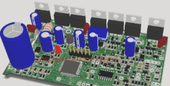
1. PCB Width, Thickness, and Components
Consider the current-carrying capacity of copper traces on a printed circuit board. Ensure attention to component height distribution, overall shape, and size. For 1oz and 2oz traces, a 10% reduction in the nominal value is permissible due to factors like etching process and temperature fluctuations. Protective coating on PCB components with specific thickness and copper foil requirements may have a reduction factor of 3. Impregnated PCBs can accept a 30% reduction.
2. PCB Line Spacing
Calculate minimum line spacing to prevent voltage breakdown between adjacent traces. Factors influencing spacing include peak voltage, atmospheric pressure, and the type of coating applied.

3. Capacitive Coupling Parameters
Place critical impedance components close together to minimize phase delay. Properly isolate transformers and inductors to prevent coupling. Position inductive signal traces orthogonally to each other to reduce interference from magnetic field variations.
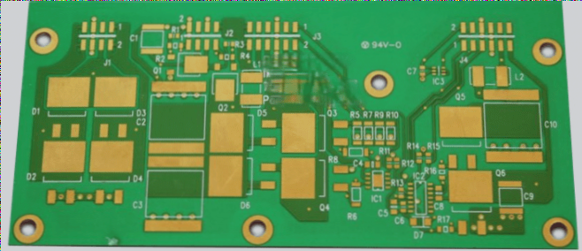
4. PCB Layout Inspection Checklist
- Are traces short and straight?
- Are trace widths within limits?
- Is minimum trace spacing maintained?
- Is parallel routing minimized?
- Are sharp angles avoided?
5. PCB Design Review Checklist
- Verify schematic accuracy.
- Confirm correct component footprints.
- Check spacing between high and low-current areas.
- Ensure schematic and layout correspondence.
- Verify proper component placement.
- Check temperature-sensitive component proximity to heat sources.
- Ensure correct transformer orientation.
- Verify connector alignment and accessibility.
- Check for missing or faulty component leads.
- Ensure vias and traces alignment.
- Properly arrange power and signal traces.
- Optimize pad sizes and solder holes.
- Place connectors near PCB edges for easy handling.
- Ensure power and ground trace width adherence.
- Optimize mounting hole size and placement.
Key Tips for PCB Design
When designing a PCB, it is crucial to pay close attention to the height distribution of components and the overall shape and size of the board. This ensures smooth and hassle-free assembly processes.
Latest PCB Design Trends
- Increased focus on miniaturization for compact electronic devices.
- Integration of IoT capabilities for smart and connected products.
- Adoption of flexible and rigid-flex PCBs for versatile applications.
Expert Advice
If you have any inquiries or need assistance with your PCB design, feel free to reach out to us at info@wellcircuits.com.