Introduction:
With the increasing use of flexible printed circuit boards (FPC) in various applications, the FPC products are poised to undergo a transformation similar to rigid printed circuit boards (PCBs). The range, types, structures, and quality levels of FPCs are expected to expand rapidly and diversify, influenced by both local and global market trends.
Flex-PCB Manufacturing Process:
Common manufacturing processes for double-sided and multilayer flexible PCBs include the following:

Materials Preparation (Blanking):
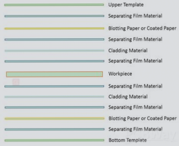
The preparation of materials for Flex-PCB involves flexible copper-clad laminates, cladding layers, and reinforcement plates. Additional materials used during lamination include separation films, conformal materials, silicone rubber sheets, ink-absorbing papers, or coated papers.
Drilling:
Due to the soft and thin nature of flexible copper-clad laminates and cladding layers, drilling can be challenging. Stacking multiple layers before drilling is necessary, resembling a book’s stacked pages.
Desmear and Pitting:
Following drilling, it’s essential to completely remove resin debris from the walls of PCB holes to ensure high-quality plated-through holes (PTH). Typically, desmearing and pitting processes are carried out before PTH.
- PTH and Pattern Plating:

- Electroless Plating:
Ideally, the pre-treatment solution should utilize acidic colloidal palladium instead of alkaline ionic palladium. Precise control of reaction time and speed is critical to prevent damage to the flexible materials and preserve the mechanical properties of the copper layer.
- Electrical Plating:
Improving Mechanical Properties of Electroless Copper Plating Layers in PCB Manufacturing
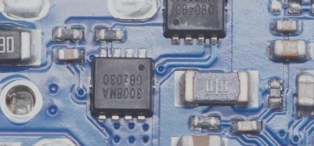
In PCB manufacturing, electroless copper plating layers are crucial components. However, these layers often exhibit poor mechanical properties, such as ductility, which can lead to vulnerability under thermal shock. To address this issue, it is recommended that once the chemical copper plating layer reaches a thickness of 0.3–0.5 microns, electrical plating should be conducted to increase the copper layer thickness to 3–4 microns. This process helps enhance the integrity of the hole wall coatings, ensuring the reliability of the PCB.
Key Steps in PCB Production Process:
- Pre-cleaning and Imaging:
Prior to imaging, it is essential to clean and roughen the PCB surface. For flexible substrates, which are prone to deformation, chemical or electrolytic cleaning is recommended to ensure optimal results. The application of dry film, exposure, and development processes should be carried out with caution to prevent warping or peeling.
Etching:
Flexible substrates often feature long parallel traces that require consistent etching. Attention to spraying direction, pressure, and transmission direction of the etching solution is crucial for uniform etching. Using a rigid substrate in front of the flexible one during etching can aid in forward movement, and an automatic regeneration system for etching fluid is beneficial.
Surface Treatment and Cladding Layer:
After etching, PCBs require surface treatment to enhance adhesion before applying the cladding layer. Drying both the drilled cladding layer and etched flexible PCBs in an oven for 24 hours before lamination is recommended to mitigate moisture absorption. The stack-up height should not exceed 25mm to maintain structural integrity.
Lamination:
- Lamination of Cladding Layer for Flex-PCB:
The lamination process for flexible PCBs is material-specific and involves controlling lamination time, heating rate, and pressure. Typical process parameters include:
1. Lamination Time: Maintain full pressure for 60 minutes.
2. Heating Rate: Reach 173°C within 10 to 20 minutes from ambient temperature.
3. Pressure: Apply 150N-300N/cm² pressure, reaching full pressure within 5-8 seconds.
Gasket Material for Lamination:
The Importance of Gasket Material in PCB Lamination
The choice of gasket material plays a critical role in ensuring the quality of both flexible and rigid-flex PCB lamination processes. The ideal gasket material should possess excellent formability, low fluidity, and minimal shrinkage during cooling to prevent bubbles or deformations.
Types of Gasket Materials
- Flexible System: This category includes PVC film, radiation-crosslinked polyethylene films, and various thermoplastic materials.
- Rigid System: Comprised mainly of glass cloth reinforced with silicone rubber.
Baking Process
The primary objective of the baking process is to eliminate moisture from the PCB during manufacturing.
HASL or Hot Melting
Following the drying phase, it is essential to subject the PCB to HASL (Hot Air Solder Leveling) or hot melting immediately to prevent moisture absorption.
Sharp Processing Techniques
Flexible PCB shaping involves the use of seamless, precision steel dies in mass production. These dies can be tailored as single-cavity or multi-cavity molds.
Packaging and Shipping Recommendations
To ensure the protection of flexible PCBs during transit, consider separating them with wrapping paper or foam pads. For enhanced safeguarding, stack multiple boards with foam pads and vacuum-seal using a vacuum packaging machine. Alternatively, utilize vacuum bags with desiccants to prolong storage life.
Shipping Options
At Wellcircuits, we offer various shipping services including FedEx, DHL, EMS, UPS, TNT, Hong Kong Post, and more to cater to our customers’ preferences.
If you have any inquiries regarding PCBs or PCBA, feel free to reach out to us at info@wellcircuits.com.