Practical Guide to PCB Fault Detection
1. PCB Failure Analysis
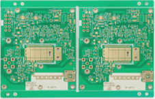
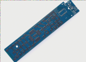
- PCB Overview: A printed circuit board (PCB) is crucial for electronic devices, ensuring consistency, automatic component insertion, soldering, and detection.
- Common Failure Factors:
- Inadequate circuit board layout causing electromagnetic interference.
- Damaged components hindering system functionality.
- Unstable component performance leading to equipment unreliability.
- Issues like solder joints causing circuit failures.
2. General Process of PCB Fault Detection
2.1 Pre-Detection Steps
- Understand the equipment’s working environment and potential electrical impacts.
- Analyze specific failures and root causes.
- Inspect critical components on the circuit board.
- Implement measures to reduce electromagnetic interference and static electricity.
2.2 Fault Detection Principles
2.2.1 Visual Inspection and Instrumentation
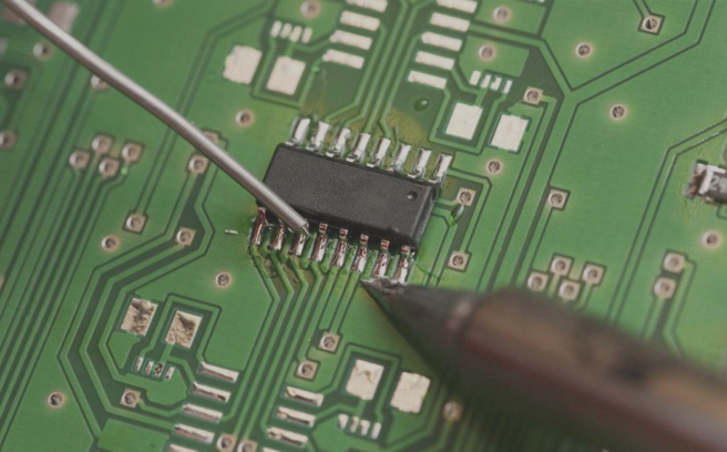
Start with manual observation and then use tools like microscopes for precise measurements. Focus on checking connections, component pins, and solder joints.
2.2.2 Component Identification
Efficiently identify problematic components as they are often the root cause of PCB issues.
2.2.3 Testing Techniques
Follow the principle of “easy first, complex later” in testing methods. Prioritize shielding against interference and testing components individually.
By following these practical steps and principles, you can effectively detect and address faults in PCB manufacturing, ensuring optimal performance of electronic devices.
Component Inspection and Testing Techniques in PCB Fault Detection
When it comes to PCB fault detection, starting with simpler components before moving on to more complex ones is a common practice. Simple components are usually easier to troubleshoot. During testing, it is recommended to use an exclusion method by testing each component individually and maintaining detailed records. If a test fails, it should be retested for accuracy. If the issue persists, documenting the result before moving on to the next component is crucial. Components that fail testing should be considered key suspects.
Supplementing Testing Methods
Relying solely on one testing method may not uncover all faults. Beginning with simpler techniques and then incorporating more advanced methods as needed is advisable. PCB testing has advanced from manual visual inspection (MVI) to online testing (ICT), boundary scan technology (BST), and now includes non-vector testing methods.
From Static to Dynamic Detection
One method involves measuring the voltage at the pins. Voltage values should vary for different pins when the circuit board is powered normally. However, factors like pin sensitivity and adjacent component faults must be taken into account. Another approach is online resistance measurement. With ICs using direct coupling, the DC resistance between the IC’s other pins and the ground pin remains relatively stable. This internal DC resistance can be measured using a multimeter to evaluate each pin’s condition. Matching the measured resistance with the reference value indicates normal IC function, while significant deviations suggest internal chip issues that may necessitate replacement. Online voltage and resistance measurements are often combined in testing.
Concluding Remarks
Presently, PCB testing technologies encompassing multiple disciplines are becoming more diverse. Each technology has specific applications; for example, online testing is limited by the device test library, while boundary scan methods have stringent requirements for reference circuit boards. To improve the accuracy and efficiency of PCB fault detection, practitioners should follow the general processes outlined here and adhere to the four detection principles. By effectively utilizing various testing techniques, PCB fault detection can be more automated, intelligent, and efficient.