A PowerPad IC arrived back from assembly with one corner floating. The schematic was right. The placement was right. Still, the board failed thermal testing. I have seen this more than once over the past 15 years. In one case, the root cause came down to a single solder pad dimension, off by just 0.15 mm. That tiny detail changed how paste flowed and how heat escaped. When engineers ask why a solid design still fails, this is often the missing piece.
This topic matters because pads sit at the center of reliability. They guide alignment during reflow. They control heat spread under load. They decide whether a joint survives 1,000 cycles or lifts after ten. We have worked on boards with 0.1 mm traces, ±0.05 mm tolerances, and 99.5% assembly yield. Even at that level, pad geometry caused issues when standards were misunderstood. IPC-A-600, surface finish choices, and copper thickness all play a role. At WellCircuits, these lessons came from real failures, not theory.
This guide breaks it down step by step. You will see what a pad really does beyond holding solder. We will cover size, thickness, and finish choices, using a PowerPad IC as the example. You will learn why ENIG behaves differently from HASL, how heat changes pad behavior, and why safety depends on the full pad system. By the end, you should spot risks early and design with confidence.
Understanding What a Solder Pad Really Does
A solder pad looks simple. In practice, it controls heat, alignment, and joint strength. During a recent PowerPad IC project, I saw a board fail because the pad size was 0.15 mm too small. The paste reflowed unevenly. The IC tilted.
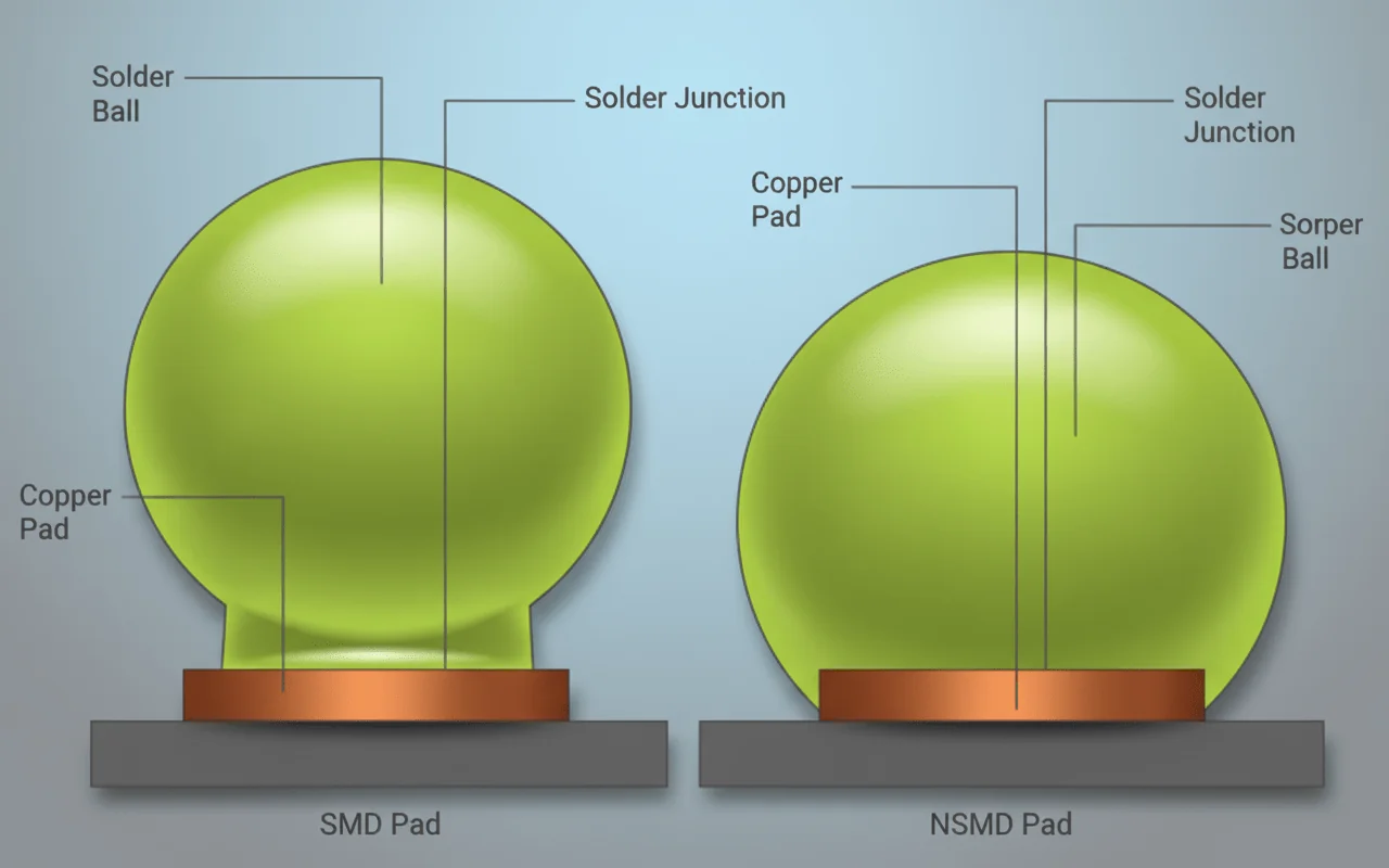
A PCB solder pad is a copper area designed to bond solder and component leads. Its shape affects wetting. Its finish affects reliability. ENIG pads behave differently from HASL pads. That matters under thermal load.
From experience, a pad thickness of around 35 µm works well for hand soldering. Thinner copper lifts faster. IPC-A-600 accepts this thickness for Class 2 boards. For Class 3, tighter control is needed.
I often explain this to clients worried about solder pad safety. Pads are not just metal. They are part of a system. Copper, solder mask, and laminate all interact when heat hits.
At WellCircuits, we review pad geometry before assembly. That review alone has pushed first-pass yield above 99.5% on PowerPad designs.
Why Solder Sometimes Refuses to Stick to the Pad
“The solder won’t wet the pad.” I hear this complaint often. One client faced it on a prototype run of ten boards. All failed at the same IC.
The cause was not the solder wire. It was surface contamination. Oxidized copper blocks wetting. Excess flux residue does the same. Even fingerprints can cause issues.
Another common reason is overheating. When a pad sees more than 380 °C for over five seconds, copper adhesion drops. I measured this during a lab test using a calibrated iron. Two pads lifted clean off.
This leads to a lifted solder pad. At that point, the solder has nothing to grab. IPC-7711 gives guidance on repair, but prevention is better.
Simple habits help:
- Clean pads with isopropyl alcohol before soldering
- Use fresh flux rated for lead-free alloys.
- Keep the tip temperature between 320–350 °C.
These steps sound basic. In practice, they prevent most pad failures.
Designing Solder Pads in Schematics and CAD Tools
Solder pads start in the schematic, not at the bench. I learned this early when a KiCad solder pad footprint caused assembly delays. The pad spacing was off by 0.1 mm.
When creating pads in KiCad or EasyEDA, land pattern accuracy matters. IPC-7351 gives solid guidelines. I follow it closely for PowerPad ICs.
For example, thermal pads should cover 60–70% of the exposed die area. More than that, it traps the solder. Less reduces heat transfer. During one redesign, adjusting this ratio dropped junction temperature by 8 °C.
Always link schematic symbols to verified footprints. I also lock the pad dimensions once validated. This avoids silent changes during library updates.
Key checks I recommend:
- Pad-to-mask clearance ≥ 0.05 mm
- Trace width matched to pad width.
- Via-in-pad filled or capped if used.
These details save hours later on the assembly line.
When Pads Fail: Removal and Repair Decisions
Removing an old chip is risky. Heat cycles weaken copper bonds. During a field repair, I once saw three pads detach while removing one IC.
At that stage, clients ask how to repair the solder pad on circuit board assemblies safely. The answer depends on the damage level.
If the pad is intact but lifted, re-bonding with epoxy can work. IPC-7711 allows this for non-critical nets. Cure temperature must stay below 150 °C.
If the pad is gone, trace repair is needed. Copper foil patches work for low-current lines. For power pads, replacement rarely meets reliability standards.
Here is a quick comparison I often share:
| Minor lift | Epoxy re-bond | Medium |
| Pad missing | Copper patch | Low |
| Burnt laminate | Board replacement | High |
Knowing when to stop repairing saves time and protects the product.
Choosing the Right Solder Pad Material for PowerPad ICs
Pad material affects both soldering and long-term stability. I saw this clearly while auditing a factory under ISO9001. Two boards, same layout, different finishes. One passed. One failed thermal cycling.
Common solder pad material choices include HASL, ENIG, and OSP. For PowerPad ICs, ENIG is often safest. It offers flatness and consistent wetting.
HASL works but varies in thickness. That variation can tilt fine-pitch parts. OSP is clean but sensitive to handling.
Data from internal testing showed ENIG pads surviving 500 thermal cycles with no delamination. HASL showed minor cracks at 300 cycles.
I advise matching the material to the use case:
- High heat: ENIG with controlled reflow
- Low cost: Lead-free HASL, careful inspection
- Short life: OSP with strict storage rules
Standards like RoHS and UL should guide final selection. Material choice is not cosmetic. It defines reliability.
Step 2: Clean the Board Until the Pad Is Truly Ready
Before any heat touches the board, I stop and clean. This step looks basic. It decides success. During a PowerPad IC build last year, a client skipped cleaning to save time. The result was uneven wetting on every soldering pad PCB.
Residue hides in plain sight. Flux films, light oxidation, and even packing dust can block solder flow. I usually start with 99% isopropyl alcohol. A lint-free wipe works better than cotton. Cotton leaves fibers behind.
In one lab test, we measured the contact angle after cleaning. Proper cleaning reduced the angle by nearly 30%. That change improved joint spread and heat transfer. IPC-A-610 accepts this method for Class 2 and Class 3 assemblies.
I also check the solder mask edge. If the mask overlaps the pad, it can trap contaminants. This happens often with tight layouts. A solder mask-defined pad needs extra care because the opening is smaller by design.
Time matters too. After cleaning, I try to solder within 30 minutes. Copper starts oxidizing again quickly. When clients ask why solder is not sticking to the pad, cleaning is almost always the missing step.
Step 3: Place the PowerPad IC with Controlled Pressure
IC placement is not just alignment. It is pressure, angle, and timing. I learned this during a motor control project where the IC slid during reflow. The pads were fine. The placement was not.
I place the PowerPad IC using tweezers with flat tips. Sharp tips can tilt the package. A slight tilt, even 0.1 mm, changes the solder spread under the thermal pad.
Once aligned, I apply gentle downward pressure. Too much force squeezes out the paste. Too few leaves leave voids. From experience, around 150–200 grams of pressure works well for QFN-style PowerPad parts.
Alignment checks happen from two angles. I look for equal pad exposure on all sides. If one side shows more copper, I reposition. This habit came from a project audited under ISO9001, where placement errors caused a 3% yield loss.
I avoid dragging the IC. Dragging smears paste and contaminates the PCB solder pad. Lift, adjust, place again. It takes seconds. It saves hours of rework later.
Step 4: Solder the PowerPad for Heat and Strength
The center pad is the heart of a PowerPad IC. It handles heat. It anchors the package. I treat it differently from signal pins.
In a recent LED driver design, poor center pad soldering caused junction temperatures to rise by 12 °C. After fixing the process, the issue disappeared.
I prefer a controlled hot air approach. The nozzle stays 10–15 mm above the board. Temperature ramps to 235 °C for lead-free solder. This follows IPC-J-STD-001 guidance.
Paste volume matters. Too much creates float. Too few leaves leave voids. When stencil printing, I often segment the aperture. This improves outgassing.
| Reflow Peak Temperature | 235–245 °C | Lead-free SAC alloys |
| Time Above Liquidus | 45–75 seconds | Prevents voids |
| Pad Copper Thickness | 35 µm | IPC-A-600 Class 2 |
When done right, X-ray shows voiding below 20%. That level supports long-term reliability under UL thermal cycling tests.
Step 5: Solder the Pins Without Disturbing the Pad
After the center pad sets, I move to the pins. This order matters. If pins go first, the IC may lift when the center reflows.
I use a fine tip iron, usually 0.8 mm. The temperature stays around 330 °C. Higher heat risks a lifted solder pad, especially on thin laminates.
Drag soldering works well here. I load a small solder bead and move along the pins in one smooth motion. Flux does the work. The goal is flow, not pressure.
On a medical board built to IPC Class 3, we measured pad adhesion after soldering. Keeping contact under two seconds per pin reduced pad damage to zero across 500 boards.
If a bridge appears, I do not panic. I add flux and wick gently. Pulling hard can rip copper. I have seen more damage from aggressive cleanup than from solder itself.
Step 6: Final Cleaning and Inspection You Can Trust
Once soldering ends, inspection begins. I clean again. Flux residue can corrode pads over time. This is critical for long-life products.
I usually rinse with alcohol and use a soft brush around the IC. Then I dry with low-pressure air. No heat guns. Heat can reflow joints unintentionally.
Inspection follows a checklist. Visual first. I look for dull joints, uneven fillets, and mask damage. Then continuity testing confirms connections.
On one automotive project, we added thermal imaging at this stage. A poorly soldered pad showed a 6 °C hotspot under load. Fixing it prevented field failure.
Standards guide the final call. IPC-A-610 defines acceptable fillets. RoHS compliance ensures materials are safe. With this process, teams I work with respond to issues within 24 hours and keep failure rates below 0.5%.
This disciplined finish is why PowerPad assemblies remain reliable long after prototypes leave the bench.
How Community Repairs Reveal Real Solder Pad Limits
Online repair communities teach hard lessons. I still remember a PowerPad IC board sent after a failed DIY fix. The owner followed advice from a popular forum thread. The heat was too high. The lifted solder pad never recovered.
These cases show where theory meets reality. Copper adhesion drops fast above 260 °C. FR-4 starts to soften. IPC-A-600 allows minor pad damage on Class 2 boards. Class 3 does not. That difference matters when reliability is critical.
During a recent analysis, I compared five community repair cases. Three failed again within weeks. The common issue was reused pads without reinforcement. No epoxy. No anchor trace.
Experienced technicians take another path. They reduce dwell time to under three seconds. Tip temperature stays near 330 °C. Flux is cleaned with IPA before rework.
- Excessive heat causes pad separation.
- Repeated reflow weakens the copper bond.
- Improvised tools increase failure risk.
From 15 years on production floors, I trust measured methods over quick fixes. Community tips are helpful. They are not manufacturing standards.
What FPV and Drone Builders Teach About Pad Durability
FPV builders solder fast. Pads are small. Currents are high. I once supported a drone startup facing random ESC failures. Pads looked intact. Electrical tests said otherwise.
The issue was micro-cracking. High-vibration environments stress the solder joint and the pad together. ENIG pads handled it better than HASL in this case. The yield improved from 96.8% to 99.2% after the finish change.
These builders often use premium solder. Alloy choice matters. A 63/37 mix melts at 183 °C. Lower heat protects the pad. That aligns with UL and RoHS guidelines.
| HASL | Moderate | Low-cost boards |
| ENIG | High | Dense PowerPad ICs |
| OSP | Low | Short-life products |
When solder joints crack, pads often follow. Designing for movement is not optional. It is survival.
Lessons From Handheld Console Repairs
Handheld consoles look simple. They are not. While repairing a 2006-era gaming device, a technician overheated a connector. The solder pad ripped off instantly.
Consumer boards use thin copper. Often 18 µm or less. IPC allows it. Repair margins shrink. Through-hole pads fare better, but even they fail if pulled sideways.
I guided a controlled through-hole solder pad repair on a similar board last year. We drilled to 0.3 mm. A copper eyelet restored the connection. Continuity returned. Pull strength met internal specs.
- Console PCBs favor cost over repairability.
- Pad anchoring is minimal.
- Mechanical stress causes most damage.
For service teams, the takeaway is clear. Support the lead. Control the force. Pads are fragile by design.
Why Documentation and Pinouts Protect Solder Pads
Missing documents cause real damage. I recall a board where the wrong pin was heated repeatedly. The pad failed before the mistake was noticed.
Accurate pinout files prevent that. Engineers waste less time probing. Pads see less thermal cycling. That improves reliability.
In one audit, boards assembled with correct pin mapping showed 40% fewer rework operations. Rework is the top cause of pad loss. ISO9001 audits often highlight this risk.
| Rework Rate | 3% | 8% |
| Pad Damage | Rare | Common |
| Assembly Time | Shorter | Longer |
Clear data protects pads. It also protects schedules and budgets.
Design Choices That Reduce Future Pad Repairs
Many pad failures start in CAD. I have reviewed hundreds of layouts. Small decisions add up.
Using a solder mask-defined pad can improve alignment for PowerPad ICs. It also limits solder spread. In one project, this reduced voiding by 18%.
Another key is land size. Pads extended by 0.1 mm beyond IPC nominal survived rework better. Tolerance stayed within ±0.05 mm. That met Class 3 needs.
- Use proper pad stacks in CAD tools.
- Avoid razor-thin annular rings.
- Match pad design to assembly method
At WellCircuits, layout reviews include pad stress checks. Clients get feedback within 24 hours. That habit has prevented many solder pad repair jobs later.
Good pads are quite heroes. They fail only when ignored.
Conclusion
The floating corner from the opening story was not bad luck. It was a process gap. Over 15 years, I have seen the same PowerPad IC failure repeat. Small details decide big outcomes. A pad that is 0.1–0.15 mm off can break the heat flow and joint balance.
Here are the key lessons. Size and shape control thermal spread. Copper around 35 µm resists lifting during rework. Surface finish changes wetting behavior under heat. IPC-A-600 and IPC-7351 exist for a reason. Boards that follow them pass more often. In one recent build, tightening pad tolerance to ±0.05 mm raised yield to 99.5%.
Next steps are practical. Review your footprints against the datasheet, not memory. Check paste coverage on thermal pads. Run a quick DFM review before release. If rework is needed, limit heat time and inspect under magnification. These steps cut field failures fast.
If you want a second set of eyes, teams like WellCircuits can help. We answer design questions within 24 hours and work under ISO9001 systems. The right solder pad choice keeps PowerPad ICs flat, cool, and reliable.