Understanding Multilayer PCB Circuit Boards
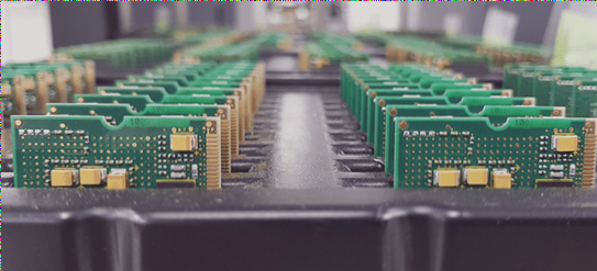
As electronic devices continue to advance in complexity, the design and production of PCB circuit boards have followed suit. Multilayer PCBs have emerged as a solution to accommodate the increasing demand for more intricate functionalities within limited space.
Key Differences Between Multilayer and Double-Layer PCBs
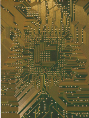
- 1. Multilayer PCBs consist of multiple layers of conductive patterns and insulating materials, interconnected through metallized holes, whereas double-layer PCBs have only two layers.
- 2. The manufacturing process of multilayer PCBs involves laminating together various single and double-sided boards, resulting in a four-layer or six-layer configuration.
- 3. Epoxy glass cloth copper-clad laminates are commonly used in the fabrication of multilayer PCBs, with a process that includes etching, blackening treatment, prepreg application, copper foil addition, and heat pressing.
Benefits of Multilayer PCBs
1. Enhanced functionality: Multilayer PCBs allow for more complex circuit designs and increased component density.
2. Improved signal integrity: The multiple layers reduce electromagnetic interference and signal crosstalk.
3. Space efficiency: By stacking layers vertically, multilayer PCBs save space compared to traditional single or double-layer boards.
Conclusion
As technology progresses, the demand for multilayer PCB circuit boards will continue to rise, offering manufacturers the flexibility and efficiency needed to meet the evolving requirements of modern electronic devices.