Lead-Free Wave Soldering Challenges and Solutions
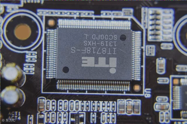
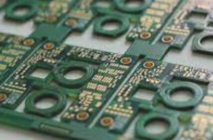
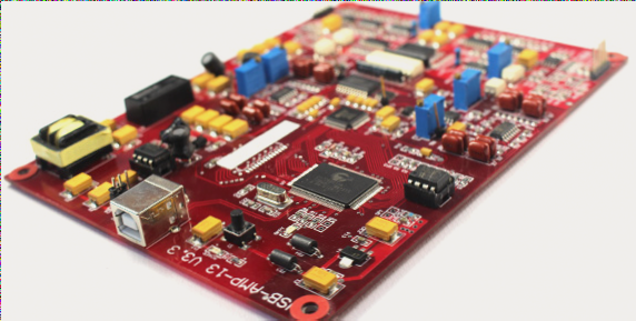
PCB components carrying electronic parts require a soldering process during assembly. Wave soldering is a common method used, but switching to lead-free wave soldering poses challenges.
Transition to Lead-Free Wave Soldering
- Preliminary estimates are made for challenges, but unforeseen issues may arise during mass production.
- Engineers continuously learn from the production process to address challenges.
- Lead-free assembly is not entirely new, having been used for years.
Adapting to Lead-Free Soldering
- Early challenges with higher soldering temperatures due to silver-tin solder have been overcome.
- Transition to lead-free components on PCBs has been smooth, with minimal process parameter changes.
- Research shows slight adjustments needed for lead-free soldering with thicker PCBs.
- Managing drainage and reducing bridging with lead-free alloys can be more challenging.
Solutions for Lead-Free Soldering
- Adjusting process parameters and using basic process control techniques can address most challenges.
- Complex PCBs with program-controlled switches require careful consideration when transitioning to lead-free soldering.