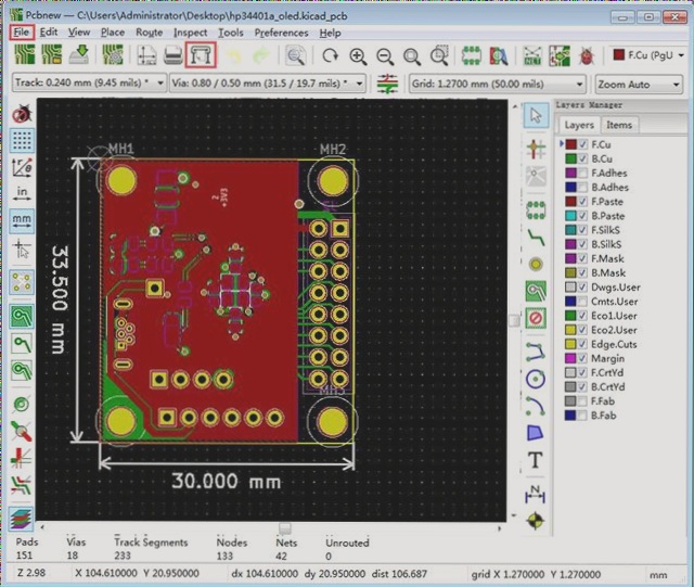
1. Opening Your KiCad .kicad_pcb File
When working on your KiCad project, simply open the .kicad_pcb file by double-clicking it within the project (.pro file) or by clicking the “PCBNew” button to access the PCB editor.
2. Creating Gerber Files from Your KiCad PCB
To generate Gerber files from your KiCad PCB, go to the “File” menu, choose “Plot,” select the required layers (for 2-layer boards), and then click “Plot” to create the necessary layers.
For a 2-layer PCB, the essential layers include:
- Top Layer: pcbname.GTL
- Bottom Layer: pcbname.GBL
- Solder Mask Top: pcbname.GTS
- Solder Mask Bottom: pcbname.GBS
- Silk Top: pcbname.GTO
- Silk Bottom: pcbname.GBO
- Drill Drawing: pcbname.TXT
- Board Outline: pcbname.GML/GKO
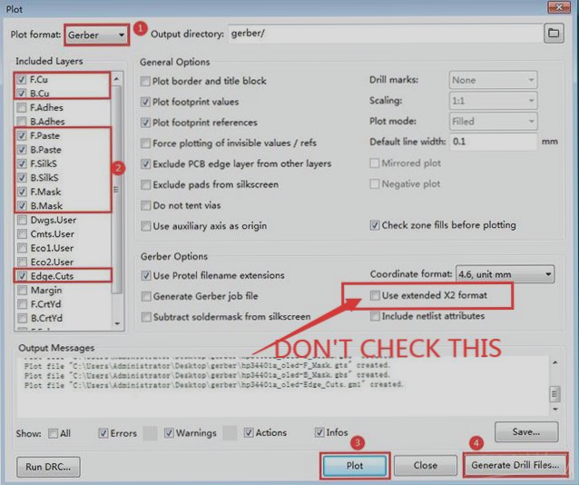
Pro Tip: To ensure easy file access, avoid selecting the “Include extended attributes” option during plotting.
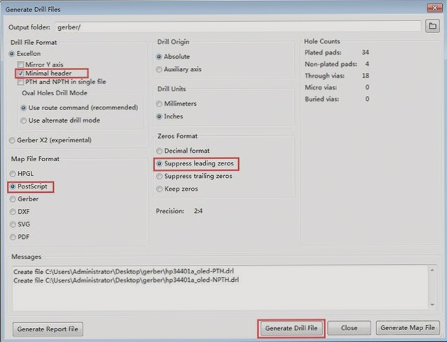
3. Generating the Drill File
Prior to closing the plot window, create the drill file for manufacturing. Opt for the “Suppress leading zeros” and “Minimal header” settings, then click the “Drill File” button.
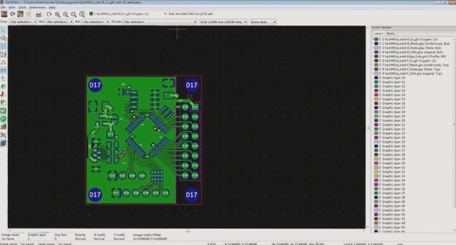
4. Verifying Gerber Files Using GerbView
After the initial steps, it’s essential to confirm the accuracy of your Gerber files before sending them for production. Use the “GerbView” tool to review the design.
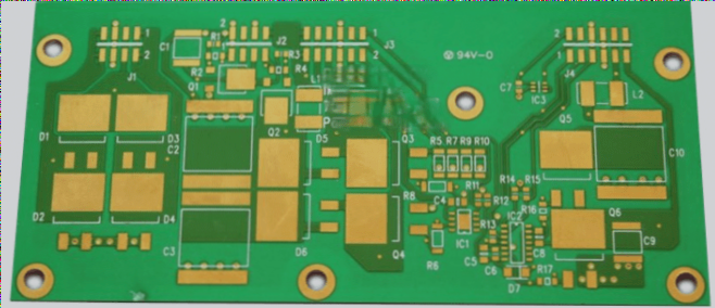
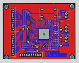
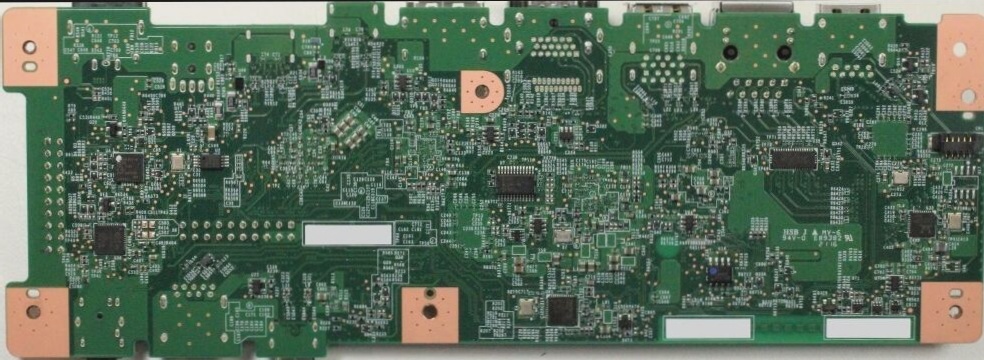
Ensure your board looks like the preview below:
5. Compiling All Files into a Single .zip File
Lastly, consolidate all necessary files into a single .zip file. Then, input your PCB specifications on our “PCB Instant Quote” page along with the uploaded .zip (Gerber) file. Our engineers will review the submission for any potential issues before fabrication.
Additional Assistance:
If you have inquiries regarding PCB or PCBA, don’t hesitate to reach out to us.